FPGAs balance architecture, IP, power in electro-optical/infrared systems
StoryMay 23, 2010


Modern Electro-Optical/Infrared (EO/IR) systems have become increasingly and exceedingly complex, and therefore demand processing capabilities best offered by FPGAs. The most critical design challenge in these systems is that of combining high-performance sensor/video processing with low power consumption. To help solve this dilemma, key sensor-processing and video-processing algorithms - and how they can be implemented on FPGAs - are presented.
Portability and versatility, coupled with leading-edge COTS technology, characterize many modern Aerospace and Defense (A&D) sensor platforms. Whether mounted on Unmanned Aerial Systems (UASs), manpacks, or left behind as autonomous sensors, Electro-Optical/Infrared (EO/IR) systems have become exceedingly complex and demand processing capabilities best offered by FPGAs. Power constraints have also tightened as a function of available energy and heat dissipation in low-footprint platforms.
These military imaging systems have become increasingly more sophisticated and incorporate multiple advanced sensors – ranging from thermal infrared, to visible spectrum, to even UV focal planes. Not only do these sensor outputs have to all be corrected (defective pixel correction and color correction) and interpolated, but images from multiple sensors must be fused, overlaid, and further processed for local display and/or for transmission on the battlefield. The key design challenge in these systems is to combine high-performance sensor/video processing with low power consumption. The following discussion focuses on some of the key sensor-processing and video-processing algorithms and how these can be implemented on FPGAs. And because an FPGA-based design reduces component count while adding flexibility, system power is reduced.
Typical sensor processing system
FPGAs are the platform of choice for almost all state-of-the-art EO/IR systems – since they meet the need for requirements for programmability, high-performance sensor/video processing, and low power consumption.
In fact, each new generation of low-power FPGAs features significantly lowers static and dynamic power consumption by utilizing a combination of architectural enhancements and lower core voltages, coupled with geometric advantages resulting from shrinking silicon feature sizes.
Sensor processing
Output from image sensors used in EO/IR systems needs correction by using algorithms such as those for non-uniformity correction and pixel replacement. While these algorithms typically require only a few mathematical operations per pixel, calculations need to be done at the pixel rate and with data that might be different for every pixel. In this case, an FPGA is an ideal platform because of the inherent parallelism in the architecture, as well as the ready availability of algorithm IP to realize video-processing functions.
For non-uniformity correction, pixel-specific coefficients need to be streamed into the logic block implementing the correction formulas. For smaller sensors, these coefficients can be stored internally in FPGA memory. Depending upon the resolution of the sensor and precision of the coefficients, the memory requirement will vary. For larger sensors, this data needs to be buffered in external memory and read out in sync with the pixel stream for every video frame. In either case, there is typically a need to change the corrective data set based on some selected parameter such as the Focal Point Array (FPA) temperature that varies greatly from ground to at-altitude.
A typical data flow for such an algorithm would double-buffer the correction coefficients to allow the relatively slow data stream from flash memory to complete before a new set of data is applied. One of the key FPGA advantages is the ability to create a data pathway that fits the algorithm, rather than change the algorithm to fit a predefined architecture. This is critical for achieving low power consumption. The massive I/O and large number of logic elements in the FPGA allow easy implementation of parallelism, and off-the-shelf IP algorithms facilitate a straightforward design. Some of the more typical sensor-processing algorithms that are available for FPGAs such as those in Altera’s Cyclone family are shown in Table 1.
Table 1: Typical sensor processing algorithms available for FPGA devices such as Altera’s Cyclone family.
(Click graphic to zoom by 1.9x)
|
|

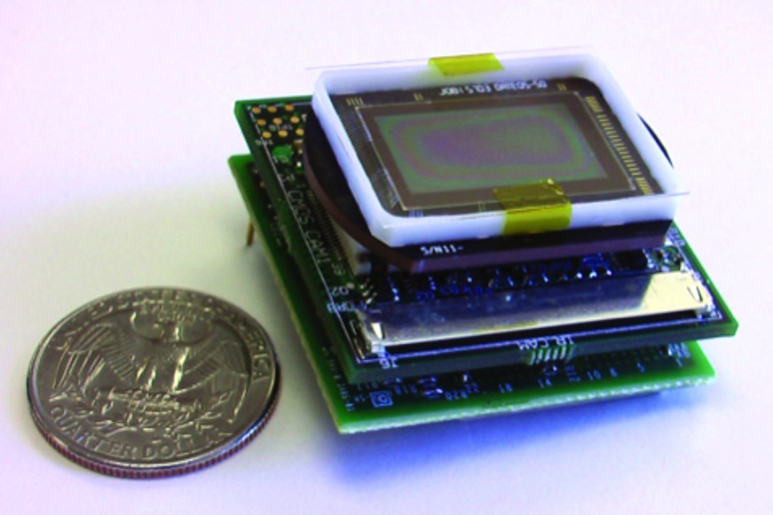
Another way that FPGAs reduce power in EO/IR sensor systems is via a dramatically lower footprint. For example, Figure 1 shows an Altera Cyclone FPGA-based system that implements a thermal sensor with integrated processing. The FPGA performs real-time image enhancement, image stabilization, and digitally enhanced resolution – and can also drive an integrated microdisplay. The FPGA power consumption in this case is ~500 mW.
Figure 1: A thermal sensor system with integrated image processing.
(Click graphic to zoom by 1.9x)
|
|
Video processing: Mixing and scaling
Military EO/IR systems often include multiple image sensors with outputs that must be fused together and displayed on a custom display with non-standard resolution. (“Non-standard” implies resolutions different from the typical desktop or laptop LCD.) A video processing system can be used to generate a composite image from two video sources on a custom display. And a video data path inside an FPGA can generate a composite image from multiple sources.
The input video is first formatted into the desired color space and is then subsequently scaled (resized) and mixed (alpha blended) with multiple other video streams. Scaling and mixing are among the most commonly used video functions, and they can be realized using off-the-shelf IP algorithms available for FPGAs.
Scaling can be as simple as copying the previous pixel (or dropping it), or it can be implemented with complex interpolation filtering techniques to generate a new pixel. Figure 2 shows the difference between the different algorithms that can be used for scaling.
Figure 2: Different video scaling algorithms and their implementation with a video scaling IP
(Click graphic to zoom by 1.9x)
|
|

The graphic illustrates all the generated pixels (shown in solid black) versus all the original pixels (shown in white). There are many ways of generating the solid black pixels; for instance, the nearest neighbor algorithm copies the preceding pixel. A more complex way would be to take an average of the two neighboring pixels in both vertical and horizontal dimension. Sometimes this is known as bilinear scaling – bilinear because it uses a pixel array of size 2x2 to compute the value of a single pixel.
Taking this concept further, one can compute the new pixel by using “m” pixels in the horizontal dimension and “n” pixels in the vertical dimension. Figure 2 additionally shows how a pixel is generated using four pixels in each dimension – also called a four-tap scaling engine.
Of course, the trick deals with the weights assigned to each pixel – also called the coefficients when realized algorithmically. The coefficients will determine the quality of the scaled image.
Figure 2 depicts one such scaling IP core available for an Altera Cyclone FPGA. This function comes prebuilt with various “Lanczos” filter functions. The Lanczos multivariate interpolation method is used to compute new values for any digitally sampled data. When used for scaling digital images, the Lanczos function indicates which pixels and in which proportion in the original image make up each pixel of the final image.
Selecting from a range of Lanczos algorithms to scale the image or bypassing them completely in favor of custom coefficients is also possible. In either case, the function automates the tedious job of generating HDL code for what is essentially a two-dimensional filter. It also maps it to the various FPGA structures such as the DSP blocks and the embedded memory blocks, thus improving productivity and reducing overall design time.
Video overlays
The other commonly utilized function is mixing and overlay of two or more video streams. This is generally done by an alpha blending function. This is a way of generating a composite pixel from two or more pixels. One pixel is assigned an opacity value called the alpha. When alpha is zero, that pixel is completely transparent (that is: not displayed). When that same alpha value is 1, the pixel is completely opaque – only that pixel is seen and the other pixel is not displayed.
In mathematical terms, the value of the composite pixel is calculated as:
C = αP1 + (1-α)P2
Where
α is the alpha value
P1 is the pixel 1 from the video layer 1
P2 is the pixel 2 from the video layer 2
C is the composite pixel
The same technique can be used to create translucent images because the alpha value can be set anywhere between 0 and 1.
A more sophisticated way of combining information from two (or more) images is to utilize image-fusion algorithms. Imagine a thermal infrared sensor and a visible image sensor depicting the same scene, but each contains information in different parts of the image.
If alpha blending could be applied to select how dominant one or the other image should be in the combined output, there would be no single value for alpha that would extract all the information available from the sensors. Figure 3 shows such a scenario.
Figure 3: Sensor fusion allows simultaneous utilization of multiple EO sensors
(Click graphic to zoom by 1.9x)
|
|

While the visible image on the top left contains information about the surroundings, the thermal view on the right only shows discernible features where there is a temperature difference against the background. Conversely, the performance of the thermal sensor is unaffected by the strong light source in the scene, while the visible camera provides no information in the same area as a result of saturation.
In the fused view, a seamless combination of information from both input modalities is achieved on a pixel-by-pixel basis. Details missing from one modality are “filled in” from the other and vice versa. One of the simplest forms of fusion would be to apply alpha blending with a different alpha value for every pixel calculated from local image statistics. State-of-the-art fusion algorithms, however, typically go beyond that and perform a decomposition of the input images that extracts relevant features around every pixel. These features are then combined to form a fused image.
Dr. Tibor Kozek is cofounder/Chief Technology Officer of Imagize LLC and has nearly 20 years of experience in signal and image processing. Prior to Imagize, he was chief scientist with Teraops, Inc., as well as a visiting scholar at the University of California, Berkeley.
Juju Joyce is Senior Strategic Marketing Engineer, Military & Aerospace Business Unit, at Altera Corporation and has more than 10 years of semiconductor industry experience. He holds a Bachelor’s degree in Electrical Engineering from the University of Texas at Austin.
Suhel Dhanani is Senior Manager, DSP, for Altera Corporation’s software, embedded, and DSP marketing group. He has more than 15 years of industry experience with Xilinx, VLSI Technology, Anadigm, and Tabula. He holds M.S.E.E. and M.B.A. degrees from Arizona State University.
Altera Corporation
408-544-7000
[email protected] • www.altera.com