CPU bypass: Critical signal processing operation
StoryJune 13, 2013

Charlotte Adams
Abaco Systems
General-Purpose computing on Graphics Processing Units (GPGPU), using massively parallel GPUs to execute thousands of math instructions simultaneously and repetitively, is a boon to signal processing. But its use in real-time scenarios has been limited...
General-Purpose computing on Graphics Processing Units (GPGPU), using massively parallel GPUs to execute thousands of math instructions simultaneously and repetitively, is a boon to signal processing. But its use in real-time scenarios has been limited by the traditional involvement of the Central Processing Unit (CPU) in Direct Memory Access (DMA) transactions.
The CPU – the heart and brains of a processing system – also can slow the system down. If the CPU has to be involved each time a data aggregator like an FPGA wants to send data to a GPU, it’s obvious that system latency increases, efficiency decreases, and system size and capability are severely limited. How would a wide area surveillance system with hundreds of imagers and multiple GPUs get target data to ground troops on time? Even more challenging, how would an aircraft Electronic Warfare (EW) system squeeze out its jamming signal in time to foil tracking radars in hostile airspace?
What’s needed is a “CPU bypass” operation, a method of data transfer – in the context of PCI Express (PCIe) – that limits, or even eliminates, the continuous involvement of the CPU in GPGPU processing. Just as coronary bypass surgery relieves the cardiac stress of clogged arteries, so a new GPU technology relieves clogged CPUs and enables GPGPU computing to serve those sensor processing applications for which it is best suited, even those with zero tolerance for latency.
A better way
Before the CPU bypass technology emerged, getting data from an FPGA into GPU memory was a roundabout process. A PCIe device first sent data into system memory via the CPU’s Memory Management Unit (MMU); the GPU then transferred the data from system memory to GPU memory. This indirect path to GPU memory added processing latency, consumed system memory bandwidth, and decreased CPU efficiency.
The new technology, GPUDirect Remote DMA (RDMA), changes this paradigm by extending DMA capability from the PCIe end points to GPU memory. Although the process uses the GPU’s MMU, it consumes no GPU cycles.
Asymmetric benefits
GPUDirect RDMA, by reducing CPU involvement in GPGPU processing, radically reduces latency. Delays can drop from 1 millisecond to as low as 50 microseconds, a decrease of 95 percent. At the same time throughput can multiply, as the unclogged CPU can manage more GPUs. The CPU now can handle as many as 16 GPUs versus a practical limit of two GPUs before.
With GPUDirect RDMA, the CPU still sets up the initial data flow from the end point to the GPU. But then the CPU can step aside and perform other operations. In a typical image processing application, for example, the GPU identifies potential moving targets in the image and gives the CPU a list of possibilities. The CPU then applies complex conditional logic to deduce probable targets in the list and initiates a transmission to a ground station.
In an EW application, however, there might not be time for the CPU to perform postprocessing tasks. In fact, the CPU might not get involved at all. The GPU could process a high volume of RF data samples from an FPGA or other sensor data collector, create the jamming signal, and send it back to the FPGA for transmission without consulting the CPU.
The key to GPUDirect RDMA is the addition of a second Base Address Register (BAR) in the PCIe end points that is dedicated to high-speed, high-volume data transfers. The CPU uses the first BAR for chores like checking the status of an end point. The second BAR, however, is larger and faster than the first, and is hooked directly to the GPU. It acts like a window into the GPU, enabling an FPGA or other I/O device to forward sensor data directly to GPU memory without GPU overhead.
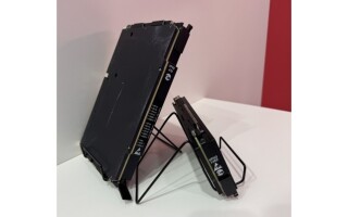
One of the first products to exploit GPUDirect RDMA is the GE Intelligent Platforms GRA112, a 3U VPX graphics card with the 384-core NVIDIA Kepler GPU implemented in individually soldered subcomponents to optimize ruggedization, cooling, and processing performance.
Figure 1: The GE Intelligent Platforms GRA112 3U VPX rugged graphics board features GPUDirect RDMA for GPGPU applications.
(Click graphic to zoom by 1.9x)
|
|

Heartsease
For real-time sensor processing applications, the benefits of the CPU bypass operation are huge. Latency plummets, GPU efficiency soars, the CPU is free to pursue other tasks, and applications previously considered to be beyond the ken of GPGPU come distinctly into view.
defense.ge-ip.com