Realizing cognitive EW in a single VPX slot
StoryApril 29, 2026

Marc Couture
Parry Labs

Electronic warfare (EW) has realized evolutionary leaps in the last decade with the fusion of several key technological categories including heterogeneous processing, high-fidelity mixed-signal converters, and the defense industry’s adoption of the Sensor Open Systems Architecture, or SOSA, Technical Standard, the C5ISR/EW Modular Open Suite of Standards (CMOSS), and VPX architectures. The continuing trend towards increased performance in a shrinking footprint has now made possible a complete cognitive EW capability in a single VPX slot with all of the associated size, weight, power, and cost (SWaP-C) and scalability benefits.
Optimizing compute performance (i.e., mission capability) per unit of size, weight, power, and cost (SWaP-C) has been a ubiquitous challenge across the defense industry for decades. Advances in processing technologies and physical form factors have enabled not only the extreme footprint compression of classic electronic warfare (EW) applications but also the addition of artificial intelligence/machine learning (AI/ML) capabilities, essential for effective deployment of cognitive EW.
Constraining the focus to the digitization of RF/IF from the analog-to-digital (ADC) converter through to the RF/IF output at the digital-to-analog (DAC), classic EW techniques have often been handled by field-programmable gate arrays (FPGAs) or application-specific ICs (ASICs) managed by a CPU processor. Plug--in-card (PIC) form factors for these systems were often VME, Compact PCI, or earlier-generation VPX profiles. Although they were based on industry standards, these systems usually integrated user-defined attributes that were hard to leverage or replace.
Even more importantly, the industry must reckon with the static nature of classic EW systems. The historic concept of operations has the EW operator selecting the appropriate EW technique based on the in-theater threat emitter. The technique would be resident in the FPGA but would be restricted to a static processing sequence with little to no adaptability. A new threat with a never-before-seen waveform would be met with no answer.
The introduction of general-purpose GPUs (GPGPUs) into embedded systems enabled the prospect of AI/ML, which has evolved countless applications across many industries – defense EW being one of them. Now FPGAs and CPUs can be tightly coupled with GPGPUs to address known threats or adapt in real time to new threats encountered during mission – in other words, cognitive EW.
The Sensor Open Systems Architecture, or SOSA, Technical Standard and the C5ISR/EW Modular Open Suite of Standards (CMOSS) reference architectures have gone farther than any other initiative to achieve a truly open ecosystem in which VPX cards from multiple vendors will actually interoperate. In particular, the introduction of blind-mate RF coax connectors and adaptable ADC/DAC daughtercards literally opens up the aperture on prosecuting the electromagnetic spectrum.
A heterogenous architecture for cognitive EW
As shown in Figure 1, an ideal heterogeneous processing mix for cognitive EW, as with many defense applications, is the triple play of CPU plus FPGA plus GPGPU. This fusion plays to the strengths of each processing category and maximizes the performance-per-unit SWaP.
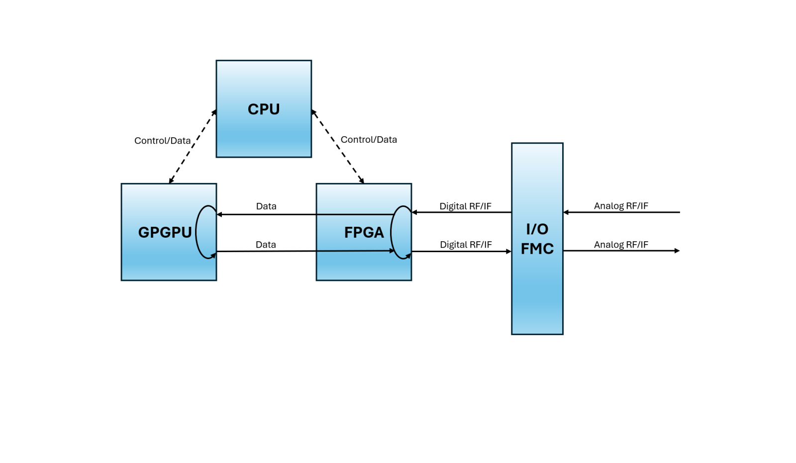
[Figure 1 ǀ A diagram of cognitive EW processing architecture.]
CPUs or GPUs [general-purpose-processors] – that is, RISC and CISC multicore processing architectures – retain their central role as overall EW application orchestrators. In recent years, advanced Arm architectures have made their way into multicore CPU packages and are even coresident in FPGA and GPGPU system-on-chip (SoC) devices.
FPGAs remain central to the execution of EW techniques, including cognitive EW approaches, due to two main attributes – extreme low latency and adaptive I/O. FPGAs are ideal for developing an EW technique in HDL optimized for timing propagation down into the single-digit-nanosecond range. Low latency, high throughput, and rigid determinism are critical for techniques as basic as range gate pull-off used in spoofing radar pulse trains. Adaptive digital signal I/O is resident on the FPGA device itself with SERDES [serializer/deserializer] or LVDS [low-voltage differential signaling], required by different types of converters depending on such factors as sampling frequencies, channel counts, and constrained latency timing through the digitizer itself.
The FPGA mezzanine card (FMC), as specified by the VITA 57 standard, is ideal for adapting to the analog RF/IF (or fiber-based digital IF) input/output channels as needed by a cognitive EW system. SERDES, LVDS timing, and other signals are fanned out from the FPGA BGA [ball-grid array] into a high-density connector that the FMC plugs into. There are many FMCs available from companies such as Epiq Solutions that house high-end MHz and GHz multichannel ADCs and DACs. With EW, the selection of converters often involves the choice of serial JESD204 or parallel LVDS with the trade being channel count versus sampling latency. Coax RF/IF cables can then be routed from the FMC to the VPX backplane as in the example of the SOSA/CMOSS software-defined radio (SDR) slot profile.
The latest participant in the heterogenous offering is the GPGPU processor, such as those from NVIDIA, which leverage hundreds or even thousands of CUDA cores and tensor cores, ideal for realizing the cognitive aspect of cognitive EW. This pool of processing cores represents a force multiplier for AI/ML workloads in addition to the DSP arithmetic often required by advanced EW techniques.
With a focus on cognitive EW data pathways as shown in Figure 1, ingress-egress loops are required to support EW techniques that require various turnaround times and adaptation feedback on radar pulse trains, communications links, and adversarial jammers. These operations all take place in the realm of micro- and nanoseconds. Taking one scenario for example: The FPGA executes techniques in nanosecond-delayed real time based on emitter threats identified in the higher-latency GPGPU, running extreme wideband frequency domain analysis of the target spectrum.
Optimal cognitive EW module architecture for VPX slot reduction
As any good systems engineer or embedded architect will contend, 3U VPX card slots are always at a premium. Slot-count reduction usually equates to reduced SWaP and cost. Cognitive EW implementations can take as many as three VPX slots to realize: One for the FPGA and FMC mezzanine, a second for the GPGPU, and a third for the multicore CPU single board computer. An additional potential issue with this architecture is that in order to increase channel count, sets of two cards at a time (assuming the CPU card does not have to be replicated) would be incrementally added when scaling up. This move can be thought of as VPX system card scaling resolution.
An alternative architecture would see the heterogenous “triple play” plus ADC/DAC digitizers all reside in a single VPX slot, meaning that cognitive EW techniques could be realized in a much smaller SWaP footprint. Scaling resolution for increased channel count and spectrum/emitter coverage would be a single 3U VPX slot at a time. This arrangement was virtually unachievable until recently.
NVIDIA GPGPU technology is an undeniable leader in the AI/ML plus DSP processing space. Of particular relevance is its Jetson system-on-module (SOM) product line which is effectively a small mezzanine assembly that includes a multicore Arm CPU plus a full GPGPU with more than 1,000 cores. This accounts for two of the three heterogeneous processing technologies required for the proposed cognitive EW architecture.
A 3U VPX baseboard is then needed that has a sizeable Xilinx FPGA, an FMC site with a mounted ADC/DAC converter FMC, and a high-density connector with space for an Orin NX Jetson SOM to plug into. The SOSA/CMOSS profile ending in 14.6.11-4 is designated as the SDR slot profile.
Figure 2 shows that the cognitive EW architecture is realized in a single SDR-based VPX slot profile supporting digital interconnectivity over the VPX backplane connectors in addition to analog signal support over VITA 67 RF/IF coax blind-mate connectors. Adjacent to the diagram is an industry example, the SOSA/CMOSS aligned Forge Boss VPX PIC.
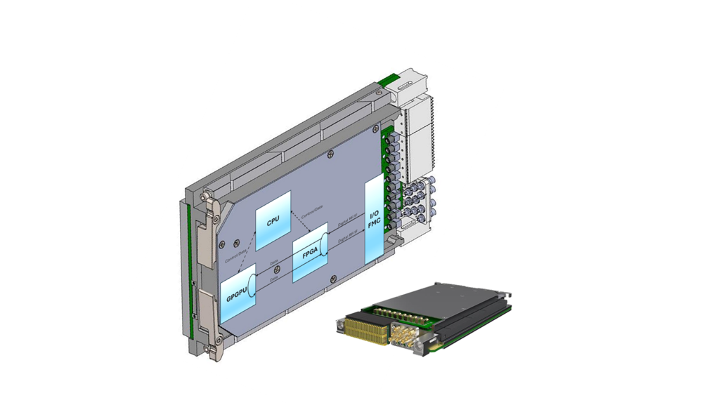
[Figure 2 ǀ A diagram shows FPGA, CPU, GPGPU, and ADC/DAC FMC in a single VPX slot next to the Forge Boss VPX PIC.]
The main engineering hurdles with this design included physical fit challenges with two mezzanines plus cable routing to blind-mate VITA 67 RF/IF coax connectors. Of relevance: There were significant thermal-dissipation challenges given the variability of FPGA IP loads and NVIDIA Jetpack modes. Finally, signal integrity was a challenge with high-speed digital signal transport and sensitive ADCs.
Advances in processing technologies and physical form factors have not only enabled the extreme footprint compression of classic EW applications but have enabled the addition of AI/ML capabilities, essential for effective deployment of cognitive EW.
Parry Labs · https://parrylabs.com/