CompactPCI solution targets rugged apps
StoryOctober 27, 2009
Jeff walks us through the features of a processor board design that was the result of efforts to stay within a desired thermal envelope yet boost performance.
One of the challenges in the architecture and design of CompactPCI processor board is staying within a “reasonable” thermal envelope. In general, “reasonable” is something under 50 W. Developers know, of course, what is available in their local computer stores, and have an expectation that solutions in the CompactPCI form factor deliver the same level of performance. This has led to somewhat of an arms race in CompactPCI processor designs as vendors strive to take the latest and greatest processor and chipset combinations and cram them onto CompactPCI designs. The results can be processor blades that approach 100 W. Fortunately, 45 nm process technology from Intel has resulted in a processor and chipset combination that will help CompactPCI stay within acceptable power levels while providing a significant increase in performance and functionality over earlier products. This article describes one example of a blade using 45 nm process technology to meet performance objectives without jumping outside the thermal envelope (Figure 1). The blade consumes less than 50 W when configured with a 2.53 GHz Core 2 Duo processor, 4 GB of memory, and a 100 GB SATA hard disk drive.
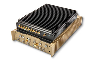
Figure 1: The cPCI-6880 blade from ADLINK uses 45nm process technology.
The Intel Penryn processor we used contains several advancements compared to the previous generation, most notably the 45 nm process technology, which enables a smaller, higher-performance die. The smaller die provides more room for a larger 6 MB cache. (In the previous generation cache was 4 MB.) The front side bus increases from 800 MHz to 1066 MHz. Intel Trusted Execution Technology (TXT) has been added. TXT is a hardware-based mechanism to protect against software-based attacks. Enhanced virtualization technology (VT-d1) improves the reliability and performance of virtualized environments. The Penryn continues Intel’s Turbo Mode support, which allows the processor to run at speeds above the rated clock frequency as long as the processor stays within its thermal envelope. Table 1 details the Penryn processor selections available with the blade.
Table 1: Intel Penryn processor selections available with the ADLINK cPCI-6880 blade
(Click graphic to zoom by 1.9x)
In addition to finding enhancements in the CPU, designers will also discover that the chipset used boasts an improved video subsystem. The graphics engine is fifth generation and runs at 533 MHz with up to 384 MB of shared memory. Hardware accelerated decode for MPEG2, VC-1, and H.264 is provided in the chipset. Supported display interfaces include single- and dual-channel 24 bpp LVDS, and DVI-I. Display resolutions are up to 1600 x 1200 for dual independent displays. The graphics performance is 30-40 percent above previous generation chipsets. Improved 3D capabilities include support for DX10 and OpenGL 2.0.
Harsh environment ready
ADLINK has made the new blade available with an extended operating temperature range of -20 ºC to +70 ºC. To withstand high-vibration environments, the blade can be configured with just the 4 GB of solder-down memory, and it contains an on-card 4 GB USB based NAND Flash. The blade also supports a conduction-cooled option.
With up to 8 GB of system memory, the cPCI-6880 has a GM45 memory controller that supports two channels of memory. The blade routes one channel to 4 GB of solder-down memory and the second channel to an SO-DIMM connector that can support an additional 4 GB of memory. The ability to handle 8 GB of memory as well as its VT-d1 support matches up well with virtualization environments. Dual BIOS PROMs provide redundancy in the event of a BIOS corruption or a need to roll back the BIOS to a previous known good revision. Other peripherals include four PCI Express based 10/100/1000BASE-T Ethernet ports, one DVI-I port, one analog CRT port, three USB 2.0 ports, a serial port, an onboard hard drive, 4 GB of NAND Flash, and a PMC site. Additional peripherals are available on the rear transition module.
The blade can do its job residing in either a CompactPCI system slot or a peripheral slot and supports 5.0 V and 3.3 V backplane V (I/O). A PCI Express to PCI bridge makes it possible for a 66 MHz 64-bit PCI interface to be used for the PMC and bridged for use on the CompactPCI bus. It is fully compliant with PICMG specifications 2.0 R3.0, 2.1 R2.0, 2.9 R1.0, and 2.16 R1.0.
Looking ahead
The continuing need to avoid thermal excess across a wide range of environments, including military and aerospace arenas, means that blades that support a 2.53 GHz processor, yet don’t cross that 50 W line, will find themselves in a ballooning market. If these same blades support 4 GB of solder-down memory, on-card NAND Flash disk, and conduction-cooled and extended operating temperature options, so much the better for an installed base that is always on the lookout for viable technology refresh.
Jeff Munch is CTO of ADLINK and heads all R&D operations in North America and Asia, and is responsible for building ADLINK’s presence throughout the world. Jeff has more than 20 years of experience in hardware design, software development, and engineering resource management. Before joining the company, he spent five years at Motorola Computer Group as Director of Engineering. Jeff is also Chair of the AdvancedTCA Subcommittee and Interim Chairman of the PICMG COM Express Plug-and-Play Subcommittee. He brings a wealth of technical knowledge and experience to ADLINK’s management team. He may be reached at [email protected].
Ampro ADLINK Technology, Inc. 800-966-5200 www.adlinktech.com


