Digital-Down Converter implementation, FPGAs offer new possibilities
StorySeptember 25, 2008

Bob Sgandurra
Pentek, now part of Mercury

Over time, Digital-Down Converters (DDCs) have shifted functionality from ASICs to FPGA IP delivery. The shift brings more optimization suited to many applications, yielding design flexibility and system-level savings. But are FPGAs always better than their ASIC rivals?
Digital-Down Converters (DDCs) have become a cornerstone technology in communication systems. Similar to its analog receiver counterpart, the DDC provides the user with a means to tune and extract a frequency of interest from a broad radio spectrum. Over the past few years, the functions associated with DDCs have seen a shift from being delivered in ASICs to operating as Intellectual Property (IP) in FPGAs.
For many applications this implementation shift brings advantages including: design flexibility, higher precision processing, higher channel density, lower power, and lower cost per channel. During the past three to four years, with the advent of each new higher performance FPGA family, these benefits continue to increase. Bob and Rich, through practical examples, explore some of these key benefits of implementing DDC designs in FPGAs – including more flexible designs and system-level savings on board count, space, and power. But are ASICs ever a better choice than FPGAs?
Digital-Down Converter fundamentals
To understand how FPGAs play a key role in implementing DDCs and performing the function of a receiver, it's important to break the DDC down into its individual functional blocks. Figure 1 shows a classic DDC. Regardless of whether it's implemented in an ASIC or an FPGA, this is a common architecture used to perform the DDC function.
Figure 1
(Click graphic to zoom by 2.3x)
|
|

The first stage of the DDC uses a digital mixer to frequency translate a specific channel frequency down to baseband using a pair of multipliers and a Direct Digital Synthesizer (DDS). This function enables the user to tune the receiver to the desired frequency of interest. The second stage of the DDC reduces the sample rate of the signal to match the desired channel output bandwidth using a Cascaded Integrator Comb (CIC) filter to decimate the data. A second CIC filter provides a coarse gain adjustment stage. The signal is then passed to a pair of additional polyphase filters: First, a Compensation Finite Impulse Response (CFIR) filter, then to a Programmable Finite Impulse Response (PFIR) filter. This filter pair provides additional decimation and final signal shaping prior to the rounding stage and final output.
When you get past all the acronyms and realize that most of the individual function blocks of the DDC are implemented using multipliers, it starts to become apparent how the DDC might map into current FPGA families. Most newer FPGAs include a wealth of DSP function blocks that are primarily multipliers. Additionally, the general-purpose logic resource and on-chip memory of FPGAs also match the requirements of the DDC for implementing the required FIR filters and filter coefficient tables.
Design flexibility: DDCs as intellectual property cores
As part of their intellectual property library series of IP, Xilinx provides a free DDC core. This Digital-Down Converter core is the basic building block of multi-channel DDCs. It follows the classic DDC architecture (Figure 1) and provides a total decimation range of 4 to 1048512. As a generic building clock, it needs to satisfy a wide range of applications and can't really be optimized for a specific range. In addition to the Xilinx core, IP is available from a number of companies providing more options and better optimization to match specific applications. Two of these cores are offered by Pentek, implemented in a Virtex-II Pro 50. The 430 DDC core is optimized for high channel count/narrow bandwidths, while the 420 core is optimized for wider bandwidths and better Spurious Free Dynamic Range (SFDR) but with fewer channels. Table 1 compares these choices with a popular ASIC-based DDC solution from Texas Instruments.
Table 1
(Click graphic to zoom by 1.9x)
|
|

When compared on a size/power/cost per channel basis, it becomes apparent that narrowband, high channel count DDC cores can be very efficiently implemented in FPGAs. Implementation of wideband DDCs tends to consume many more FPGA DSP and logic resources, limiting the number of channels that can fit in a single FPGA, thus reducing the overall savings. But even with less cost-effective wideband DDCs, the custom IP approach can sometimes provide the only viable solution when a specific performance characteristic is required like extended SFDR, for example.
IP enables flexibility in software radio products
Aside from stand-alone IP cores available from Xilinx and other IP vendors, some vendors are offering FPGA-based integrated communications receiver products that offer the IP preinstalled. As stated earlier, custom IP or cores can be optimized to address a specific application, enabling more efficient use of FPGA resources and yielding better performance.
The flexibility this optimized core approach delivers becomes more apparent when products are provided by the same vendor and are actually the same hardware with only changes to the IP core. A system engineer can design a single hardware receiver product and use it across a range of different application spaces. Additionally, some single applications, like Joint Tactical Radio System (JTRS), need to operate across a wide spectrum to handle diverse signal types. Figure 2 shows three optimized cores versus a non-optimized core across a range of applications, and the number of channels and bandwidths they typically require. Again this wide range of applications can be satisfied by using the same hardware, but different, optimized IP cores. This is one of the fundamental concepts of Software-Defined Radio (SDR), and is difficult or sometimes impossible to achieve with ASIC-based solutions.
Figure 2
(Click graphic to zoom by 2.3x)
|
|

System-level savings
So let's take a look at a complete receiver system. One common application is GSM 2G, a high channel count, low-bandwidth system. An E-GSM receiver requires 174 channels spaced 200 KHz apart. Just three or four years ago, a viable solution would have used TI/Graychip four-channel 4016 ASIC-based DDCs.
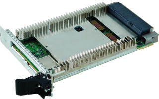
A common board form factor for these types of applications is PMC, a compact I/O module for VMEbus systems. One PMC can house two 100 MHz A/Ds and four 4016s and all of the required interface and support circuitry. For a 174-channel system, this would require 11 PMC modules. By comparison, an IP DDC with 174 channels and similar performance to the 4016 can fit in a single Virtex-5 XC5VSX95T FPGA that can be housed on a single PMC, along with two channels of 200 MHz A/Ds and all support circuitry. The PMC board count, along with cost, space, and power, can be greatly reduced as shown in Figure 3.
Figure 3
(Click graphic to zoom by 2.3x)
|
|

FPGAs versus ASICs
FPGAs continue to offer new possibilities and performance when addressing processing tasks like Digital-Down Conversion. With each new generation of higher-performance FPGAs, processing precision continues to increase, enabling IP-based DDCs to outperform their ASIC-based cousins with specifications like better Spurious Free Dynamic Range.
From a system-level view, it's easy to understand how packing many channels of DDCs into one or two FPGAs can reduce the board count, power requirements, and cost over a solution that requires 30 or 40 individual ASIC DDC chips to run the same application. Additionally, FPGA solutions can be extremely flexible by supporting vastly different signals with the simple load of an IP core and reusing the same hardware platform.
However, FPGAs are not a perfect match for all requirements. They show the greatest advantages in systems with high channel densities and typically narrower bandwidths where many DDC channels can fit on a single FPGA. In systems with just one or two channels and very wide bandwidths in the range of 100 MHz or greater, the higher cost of the FPGAs needed to fit the larger wideband DDC cores can quickly exceed the cost of designing the system with a single multi-channel DDC ASIC.
So, while cost, size, and power are important factors in designing a receiver system, ultimately the technical requirements may dictate the choice of whether an ASIC or FPGA is used.
Richard Kuenzler is a senior design engineer at Pentek, specializing in the development of DSP, I/O, and software radio hardware products. During his 17 years in the DSP industry, Rich also worked for Hughes and Raytheon where he specialized in image processing and the development of military night vision systems. He holds a Bachelor's degree from Syracuse University and has been published in various electronic industry magazines. He can be contacted at [email protected].
Robert Sgandurra serves as senior product manager over Pentek's DSP, data acquisition, digital receiver, and software products. He joined Pentek in 1994, working as an application engineer and system integrator, taking on the responsibility of product manager in 1997. Prior to Pentek, he worked seven years in the medical electronics industry designing and managing projects for ultrasound imaging. He holds a BSCS from the New York Institute of Technology. He can be contacted at B[email protected].
Pentek, Inc.
201-818-5900
www.pentek.com