Flexible military radios balance SWaP, cost specs
StoryOctober 03, 2014

Paul Dillien
Lime Micro

Over the last decade, engineers working to create software-defined radio (SDR) systems have found it challenging to design a very flexible wireless system that meets the military's requirements for space, weight, and power (SWaP) at an affordable cost.
The SDR sector was given a big boost when the U.S. military Joint Tactical Radio System (JTRS) program was initiated in 1997. The program’s ambitious objective was to allow mobile ad hoc networks to link together disparate wireless systems from the various branches of the military, other NATO armed forces, legacy radios, and some civilian systems. These systems included ground mobile radios (GMR), ground-to-air, and satellite communications.
The JTRS specification featured a wide range of what were termed “waveforms” that would be modulated onto any RF frequency over a huge range from high frequency (HF) to ultra-high frequency (UHF). The spec’s physical layer included orthogonal frequency division multiplexing (OFDM) and wideband code division multiple access (WCDMA) technologies to enable users to communicate via voice, data, and video simultaneously at all levels of security. The system was designed to support the need for mobile Command, Control, Communications, Computers, Intelligence, Surveillance and Reconnaissance (C4ISR) and to stay connected in the chaotic environment of a battlefield by using a self-healing network.
These technologies required complex processing of the baseband signal to realize the various waveforms. In order to achieve both the speed of processing and low power consumption, the design requires some form of hardware acceleration. The two most suitable options would be a hardwired mask programmed gate array or field programmable logic, such as a field programmable gate array (FPGA). The advantages of the “classic” gate array include optimized performance and low power; however, once the design is committed to silicon it has permanently fixed functionality. Moreover, non-recurring engineering (NRE) costs have escalated dramatically for leading-edge technology, due to the long production timescales typical of defense procurement. The FPGA option provided a flexible logic fabric; because it is reprogrammable, it allowed design iterations to be tested in hardware with no NRE.
The RF challenges also proved to be very difficult. The design of an RF chain that could span a wide range of frequencies is far from easy, with different frequencies requiring tunable components and an agile antenna. The bandwidth required for voice is much narrower than that needed for video, which gave added complexity to the design. Fast frequency hopping, spread spectrum, or OFDM further compounded the problems.
Unfortunately, the specification proved too complex and difficult for the technology of the day and the JTRS program was finally cancelled in late 2011. The program also suffered from feature creep and bloated requirements during the 15 years of development, which rendered much of the earlier work obsolete. When the cancellation of the program was announced, the Defense Undersecretary was quoted as saying, “Our assessment is that it is unlikely that products resulting from the JTRS GMR development program will affordably meet service requirements, and may not meet some requirements at all. Therefore termination is necessary.”
JTRS program elements live on
Fast forward to 2014: Many of the requirements from the JTRS program remain relevant today.
The advance of Moore’s Law has been relentless, so that FPGAs fabricated using 20-nm planar technology are currently shipping, with 14-nm Tri-Gate (FinFET) technology just around the corner. This update has dramatically boosted both complexity and performance. For example, the midrange Altera Arria 10 SX family expands to 660k logic elements, alongside well over 40 Mbits of on-chip memory and more than 1k DSP accelerators. The 20-nm SX devices also feature dual high-performance ARM processors.
A question: How could a designer use an Arria 10 device to meet the baseband requirements of an SDR? The first decision is to partition the tasks between the software running on the ARM processors and the hardware accelerators and interfaces that will be built in the logic fabric. The general rule is that compute-intensive functions, such as Fast Fourier Transform (FFT) encoding and decoding or Forward Error Correction (FEC), are typically more efficient in hardware. The processor is ideal for activities like data moves to memory and protocol checking and manipulating.
The equivalent of baseband “waveforms” would be various modulation standards. These could be OFDM, which demands complex FFT computations, or Code Division Multiple Access (CDMA), requiring fast spreading code generation and correlators to despread and recover the received data. The DSP blocks in the Arria device form a key element of the hardware accelerator. Modern modulation systems use data in the form of In-phase (I) and Quadrature (Q) bitstreams; this allows the RF carrier to be modulated with quadrature amplitude modulation (QAM) such as 16 (up to as high as 256 QAM), or the simpler quadrature phase shift keying (QPSK). This high-performance task can be implemented in the DSP and logic fabric to save overall system power.
The latest standard is called Multiple-Input Multiple-Output (MIMO), a complex scheme that uses two or more antennas separated by a physical distance. MIMO techniques improve the spectral efficiency and achieve a diversity gain that improves the link reliability. It is expected that MIMO will become an important addition to meet the growing demand for data throughput.
A programmable logic solution offers significant additional advantages. The logic function is defined by a configuration file held in nonvolatile external memory and loaded into the device on power-up; the memory also holds the executable code for the ARM cores. This solution allows the functionality to be updated as a midlife software update, as users could, for example, support new waveforms in the logic or add new features to the ARM code.
The ARM processors can control the data flow into the FPGA cores, using them as specially customized peripherals. As an example, one core may be allocated to controlling the interfaces, such as a display or video screen, while also verifying that the received data packets are valid (see Figure 1). The second processor can control the hardware accelerators built from the logic and DSP resources. The ARM can select the hardware accelerators that implement the algorithm currently required, for example, to produce QAM16, and to regulate the data transfer to and from the field programmable radio frequency (FPRF) chip.
Figure 1: An FPGA controlling the SDR logic.
(Click graphic to zoom)
|
|

The ARM can control the FPRF device as well with a simple and fast SPI interface using a two-byte instruction to give it complete control of the RF domain. The processor can also process the received signal strength indicator (RSSI) that indicates the activity level at the chosen frequency. The combination of the FPGA and FPRF devices provides a highly flexible, low power, and above all, cost-effective solution to the logic and RF domains.
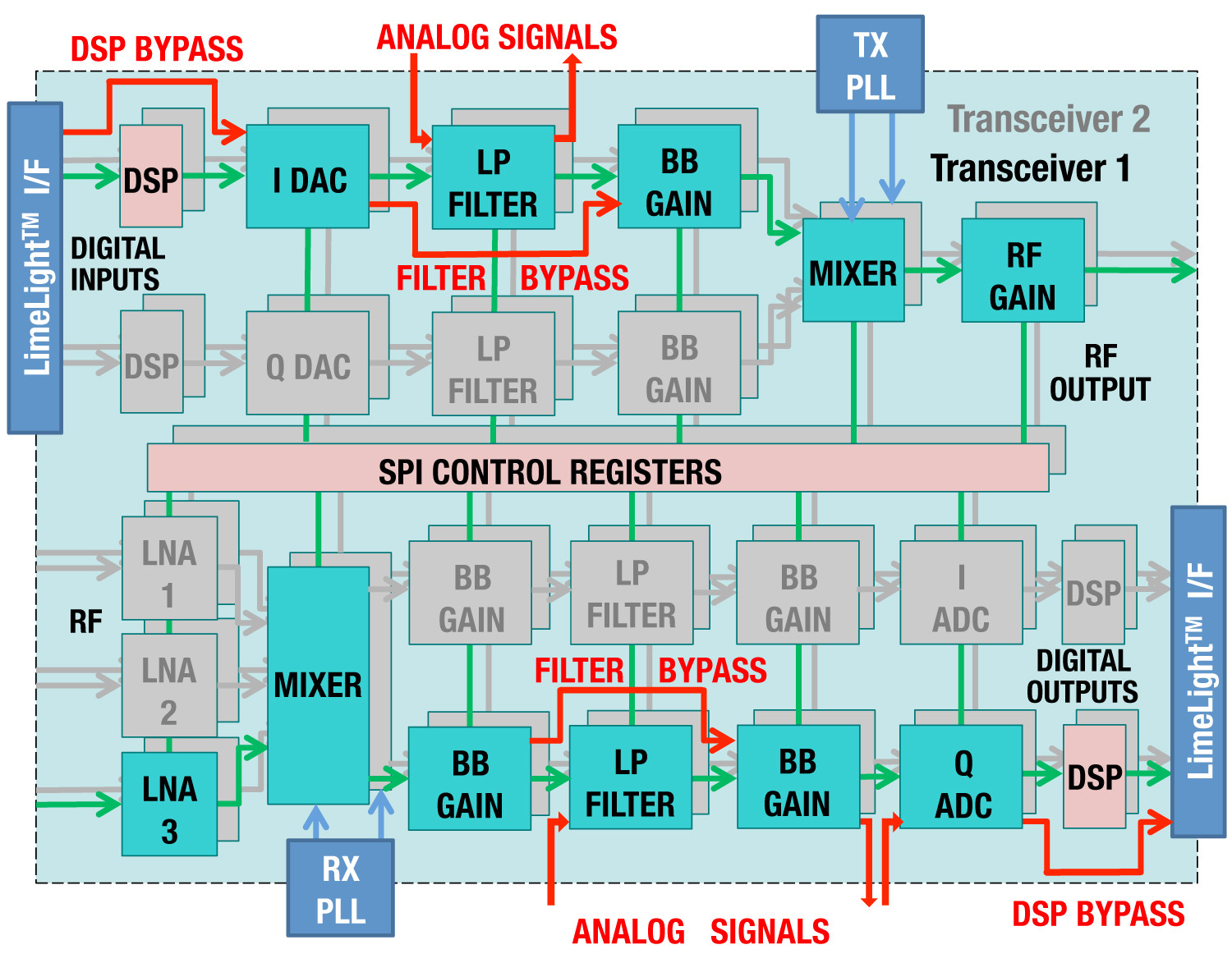
The LMS7002M, the second-generation FPRF device from Lime Microsystems, is a newly announced 65-nm CMOS chip that features a dual-transceiver architecture. The frequency range has been extended, so that it now covers 50 MHz to 3,800 MHz, giving support to the lower frequencies often used in legacy military radios. In addition, the upper limit can be easily extended with the addition of an external PLL and mixer, so that it can cover frequencies used in satellite communications.
The LMS7002M includes an on-chip microcontroller; this setup simplifies the calibration of the chip, which otherwise would involve complex interactions with the baseband logic. It calibrates DC offset, the TX/RX LPF bandwidth tuning, transmit local oscillator leakage feed-through, IQ gain and phase mismatch in both transmit and receive chains, as well as handling on-chip resistor and capacitor calibration. In most applications the initial calibration is sufficient; however, for military wireless systems operating at extreme temperatures and frequencies, then the microcontroller can be instructed to recalibrate to ensure optimum performance. Power-saving features include the ability to selectively power down any block when not required, with settings and calibration retained if power to the SPI memory is retained (see Figure 2). The FPRF chip is housed in an 11.5 mm x 11.5 mm package.
Figure 2: Each FPRF block can be selectively depowered or bypassed.
(Click graphic to zoom)
|
|
Various tools are available to help designers, either provided by the FPGA vendor or third-party suppliers. For example, Altera is the only FPGA vendor to offer a publicly available, Open Computing Language (OpenCL)-conformant software development kit. OpenCL allows programmers to take OpenCL code and rapidly exploit the massively parallel architecture of an FPGA. It enables kernel code to be emulated and debugged, pinpoints performance bottlenecks, and profiles and recompiles to a hardware implementation. The FPRF design tool from Lime Microsystems takes the form of a graphical user interface (GUI); the GUI is available free of charge and allows complete control of the device.
Paul Dillien has worked with Lime Microsystems covering a range of marketing projects for the past two years. He previously worked in the FPGA industry for 15 years, and is the author of “The FPGA Market” report. Paul has worked in strategic and tactical marketing roles for leading U.S. and U.K. semiconductor companies and specializes in competitive analysis and negotiation. Readers may reach him at [email protected].
Lime Microsystems
630-208-2700
www.limemicro.com