Mission-critical power start-up demands perfect performance every time
StoryNovember 23, 2017


Design of a mission-critical, rapid-start, isolated power system needs to be flawless. These systems, leveraged in mission-critical military applications, need to start in milliseconds - every time.
The purpose of the power supply in an electronic system is to provide a regulated voltage and/or current to a load. Attention is given to the performance of the power system in its response to rapidly changing loads and to rapidly changing voltages demanded by the load. The input voltage and start-up time of the power system is given much less consideration because it is generally assumed that the power source to the system is always present.
However, there are systems where the power source isn’t present and the system must be active within milliseconds (ms) of application of input power. These systems typically require isolation from the power source to keep grounds isolated or to meet military specifications such as MIL-STD-704, which defines a standardized power interface between a military aircraft and its equipment.
For example, in many missile-launch systems, the target information isn’t programmed into the missile until moments before launch. There are several systems that need to be active within the missile before target information is loaded; the power system is only one of these systems, and it needs to be the first system that is active to drive all the others. Therefore, the power system must get it right every time.
Designing mission-critical power systems
There are a few critical areas of consideration when designing an isolated power system that must start within 10 ms from application of input voltage. The input dv/dt should not exceed the ratings of the power components, the input capacitance cannot cause the sourcing components to exceed their ratings, and the output capacitance value should be selected such that the system does not go into current limit or exhibit instability.
The input section of many DC/DC converters includes an LC filter. If this LC filter is hit with a step voltage – that is, application of DC to the power system – the LC filter can ring up to a voltage level that can damage the internal circuitry of the power component. A common specification for maximum input dv/dt is 10 volts/microsecond. A mechanical switch or field-effect transistor (FET) that closes too quickly can easily exceed a 10-volt/microsecond rise time. An input filter with current limiting would keep the input to the DC/DC converter within its input dv/dt specifications.
Figure 1 shows the power system block diagram and Figure 2 shows the block diagram of the internals of a typical input filter. The input to a regulating DC/DC converter typically needs an input capacitor because it needs to see low source impedance and insure converter stability over line and load changes. This capacitor needs to be charged slowly as to not exceed the maximum dv/dt, but fast enough to help achieve the less than 10 ms start-up time of the power system. Starting at the application of system input voltage, Q1 in Figure 1, is off. At the undervoltage turn-on level the Charge Pump/Control block in Figure 1 will begin to enhance Q1 and raise the output voltage of the filter. This output voltage rise is controlled to not exceed the input dv/dt of the converter as well as control current drawn from the source.
Figure 1: Power system block diagram
|
|
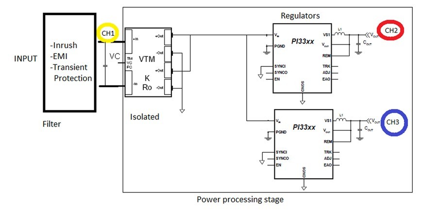
Figure 2: Internal workings of a typical input filter.
|
|

Capacitance: important factor in rapid power start-up
To aid in achieving a less than 10 ms start time the filter must charge its output C as fast as possible. Selecting the lowest value of this output capacitor is best when designing for a fast turn-on time. Using an unregulated isolator at the output of the filter would be best because these require little to no input capacitance, they don’t regulate, and thus don’t affect the control loop. A good input filter will also include EMI and transient protection to meet MIL-STD-461 standards for EMI and MIL-STD-704 and MIL-STD-1275 for input transients.
If an isolator is used at the output of the filter and the filter output rise time is controlled, then the output of the isolator will be controlled. The isolator’s output mirrors the input by the voltage ratio of the converter. This will keep the downstream regulators shown in Figure 1 within their input dv/dd specification range. The regulation stage does need input capacitance for source impedance requirements and stability, so this needs to be taken into account when determining capacitance seen by the filter. The isolator will reflect its output capacitance to its input and this will be seen by the input filter.
The capacitance reflection is the isolator’s output/input voltage ratio squared, multiplied by the isolator’s output capacitance. If the output/input voltage ratio is 1/2, and the isolator’s output capacitance is 47µF then the reflected capacitance to the filter is 1/2 squared, times 47µF or 11.75µF. The performance of the isolator is critical in this application. The isolator needs to have very little inductance as part of its power train. The low values for inductance enables current to flow rapidly from input to output while maintaining a fixed input to output voltage ratio. Some isolators have power train internal inductances in the nH range.
The input filter also keeps the source from exceeding its maximum current ratings. As an example, during a high dv/dt event such as a hot plug, mechanical switch, or FET switch closing, the filter will shield any capacitance from seeing this high dv/dt. The power system source always has a maximum current rating due to source capability, connectors and traces that go to the power supply. If these components see higher current levels they can fail or become weakened and turn into latent failures. In power systems that require less than 10 ms start-up, the input voltage to the supply must come up quickly as this timing is part of the 10 ms start-up. A quick start-up into capacitance will result in high inrush current. The filter helps to reduce this inrush. Many filters have inrush ratings in Amps per output µF. If the rating is 0.007A/µF and you have 47µF at the filter’s output then the inrush current is 0.007A*47µF or 0.329A.
In many applications, the power supply will have its own output capacitance as well as load capacitance. This capacitance is charged by the output voltage of the converters. When designing for a less than 10 ms start time the output voltage rise across the output capacitance must not cause the converter to exceed its current maximum, resulting in shut down or output voltage dip due to current limit. If the converter shuts down and restarts then the start-up time is lengthened. If the converter goes into current limit then the output voltage drops, resulting in a longer rise time and extension of the start-up period.
Taking this into account, it is best to design using the smallest amount of output capacitance possible. The output current charging the output capacitance is determined by the equation: I = C* dv/dt, where I is the converter output current, C is the output capacitance, and dv/dt is the converter output voltage rise time. If the load is active during the rise time, then this needs to be added to the current supplied by the converter. In either case, the current should not exceed current maximum. If the current does exceed the maximum, then another converter in parallel can be added to boost the current rating of this output.
The output capacitance of the converter helps keep the converter output ripple low and helps keep the converter stable during operation. Using a converter with a high switching frequency will help with keeping the output capacitance low. The high switching frequency will allow the design to use low values of inductance and capacitance to maintain output ripple as low as 30 mV to the load. Typical switching frequencies are in the 500 KHz to 1 MHz range.
When designing a power system for less than 10 ms start-up as shown in Figure 1, there will be several components that must become active and stay within each component’s power, voltage, and current ratings. When the system input voltage is applied, the filter controller must wake up and begin controlling the filter’s output voltage, keeping the source current below its maximum, and keeping the downstream converters within their maximum input dv/dt. When the downstream converters reach their undervoltage turn-on level, their internal controllers must wake up and effectively control their output voltages, charging the output capacitance, and in many cases the load current demand.
These wake-up times are cascaded; the resultant wake-up time has to be less than 10 ms. Figure 3 shows the performance of a power system configured for a less than 10 ms start-up time. The system is configured with an isolator and two nonisolated regulators. The isolator enables the system to have a separate ground between input and output. The regulators are starting into a load of 25 watts and 33 watts, while the start time from application of input voltage is measured to be around 4 ms. This system is very scalable, simply by adding power components in parallel or using components with higher power levels. Adding components in parallel also enables redundant operation.
Figure 3: A power system configured for a start-up time of less than 10 ms.
|
|

Designing an isolated power system with less than a 10 ms start-up time is achievable and reliable when using the right components. Those with high efficiency and small size makes them perfect for many military applications.
David Berry has a Bachelor of Science degree in electrical engineering from Union College in Schenectady, New York. He was a former magnetics designer specializing in impedance matching transformers; he now works for Vicor Corp. as a principal applications engineer. He has been working in component power design for 20 years.
Vicor Corp. www.vicorpower.com