Designing a general-purpose FPGA DSP card for EW, radar applications using the latest generation of FPGAs
StoryJanuary 29, 2014

Denis Smetana
Curtiss-Wright

Designing a general-purpose FPGA card that addresses the universe of Electronic Warfare (EW) and radar applications is a challenge. For any individual application, defining the requirements of the system and determining the optimal architecture for that particular solution is fairly straightforward. However, the problem is much more complex when trying to target a wide spectrum of use cases with a single FPGA module. The goal is to provide a flexible architecture that also enables the use of the latest FPGA features.
The primary purpose of an FPGA card in a DSP system for EW and radar applications is to perform front-end sensor processing, which requires a high level of parallel processing as well as adequate and flexible I/O. To process and/or generate “real” data, the DSP system must convert analog and digital data using an Analog-to-Digital Converter (ADC) or a Digital-to-Analog Converter (DAC). Conversion can be done on the FPGA board, on a mezzanine card, or on a separate board. If conversion is done on the FPGA board, the ADC/DAC processing parameters – such as sampling rate, resolution, ENOB, and SFDR – are limited by its components and can’t be changed easily. This approach, however, may simplify thermal management and often offers higher performance. Conversion on the FPGA board is preferred if the performance requirements can’t be met using a mezzanine card; for example, if the connector from the mezzanine to the FPGA board is unable to handle the required bandwidth.
A more flexible option is to provide mezzanine sites on the FPGA card. VITA 57.1 FMCs (FPGA Mezzanine Cards) enhance an FPGA board with an open-standard, high-density, highly configurable interface for FPGA I/O. Popular with designers of FPGA boards for DSP and EW applications, the FMC approach delivers access to numerous off-the-shelf ADC, DAC, or mixed ADC/DAC mezzanine card options. The third option is to use a separate, dedicated board for FPGA I/O, sending converted data to the FPGA board via serial interfaces such as SFPDP or 10 GbE. Using this approach, the FPGA board requires a high number of SERDES (Serializer/Deserializer) connected to the backplane. Today’s newest FPGAs feature numerous >10 Gbps SERDES to facilitate this capability.
EW applications require an extremely low latency path between the incoming signal to the ADC and the outgoing signal to the DAC. To minimize latency, the incoming signal path should traverse through a single FPGA. This can be accomplished by using one of an increasing number of mixed ADC/DAC FMCs and mixed ADC/DAC monolithic boards available today. Alternatively, two mezzanine sites can be connected to a single FPGA. Because round-trip latency is not usually as critical for radar, ADC/DAC functionality can be separated. Channel synchronization, sampling rates, and resolution can vary for EW and radar applications, making a configurable ADC/DAC front end the optimal design solution.
FPGA processing relies on I/O, memory bandwidth
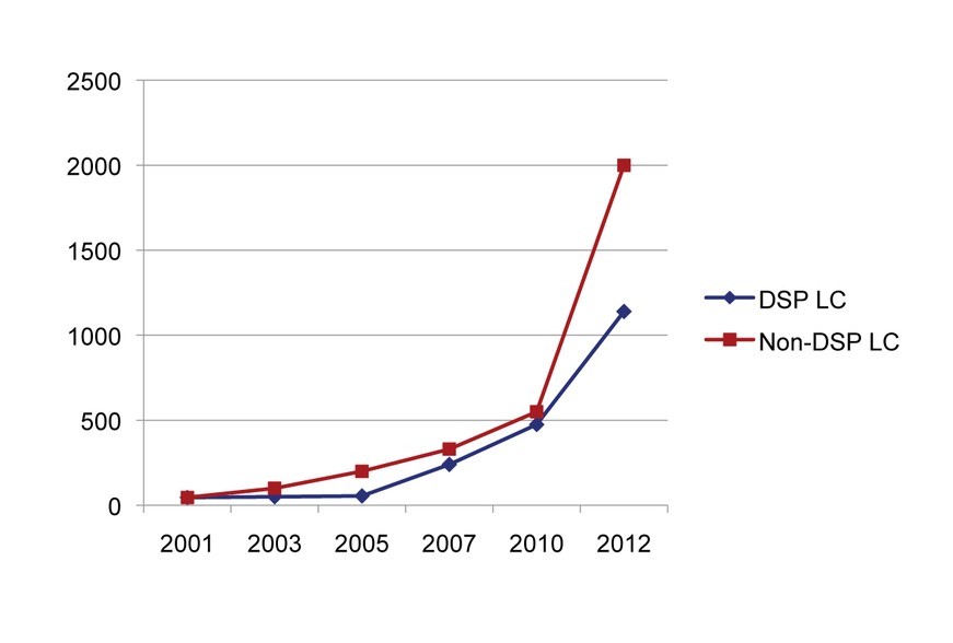
Each new generation of FPGAs increases speed, gates, and memory, and adds new capabilities. Figure 1 shows the approximate growth of logic cells delivered by recent generations of FPGAs.
Figure 1: Approximate FPGA logic cell growth for both DSP-centric and non-DSP-centric FPGAs.
(Click graphic to zoom by 1.9x)
|
|
An FPGA board designed to support both EW and radar applications requires a balance between I/O bandwidth, internal processing capability, external memory bandwidth and type, and interconnect options. If the I/O bandwidth or memory bandwidth is insufficient, then the increased FPGA processing capability cannot be fully utilized.
FPGAs and memory types
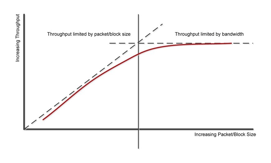
Generally, EW and radar FPGA applications require two types of memories: SDRAM for large bulk-data capture or delay chains, and SRAM for low latency or random access functions. SDRAM memory has high latency, while SRAM memory has a significantly lower capacity. The best approach for a general-function FPGA product is to use both types of memory, while also providing sufficient bandwidth for the I/O. In this capacity it is important to remember that if data is flowing through memory, the combination of writes and reads will effectively halve the available memory bandwidth. This slowdown is documented in Figure 2. Furthermore, optimal use of memory bandwidth depends on the block or packet size, which can be affected by DMA capability – something that is particularly true for high latency SDRAMs. Algorithm designers need to consider actual memory bandwidth when architecting data flows.
Figure 2: Typical throughput graph relative to packet/block size.
(Click graphic to zoom by 1.9x)
|
|
Both EW and radar applications are heavily DSP-centric, which means that in addition to using general-purpose logic, they can benefit greatly by having access to dedicated, hard-routed DSP resources. The latest FPGAs are ideal for these applications. The largest DSP-centric FPGAs contain thousands of hardened DSP blocks, containing optimized multiply-accumulate functions, and can perform more than five trillion fixed-point multiply-accumulate operations per second.
High-speed interconnect to handle data
At some point in the EW or radar application, the data on the FPGA card will need to be interconnected to other FPGA cards or processor cards. An industry-standard, high-speed interconnect – such as SRIO, PCIe, or 10/40 GbE – needs to be used so that the processor can handle the data. The newest FPGAs include Gen3 PCIe cores, and sometimes 10/40 GbE cores as hard macros, which help free up more resources for DSP functionality. It is also important to have Direct Memory Access (DMA) capability to send large blocks of data, thereby minimizing packet overhead. In-band interrupt capability is also desirable to minimize processing overhead and maintain data coherency.
For interconnecting FPGAs, a low-overhead protocol such as Aurora is usually the best option, as the speed is not limited to a specific frequency and can be adjusted as needed. In some applications, the ability to decouple the transmit and receive SERDES with Aurora is beneficial, because the transmit and receive links can then be daisy-chained from one FPGA to another.
As backplane architecture speeds reach 10 GHz, many techniques need to be implemented to ensure good signal integrity. These techniques include the correct selection of low loss, the use of smooth-weave PCB material, sufficient signal isolation, back drilling of vias to manage stub length, and the minimization of trace impedance mismatches. See Curtiss-Wright’s new white paper, “The Importance of Signal Integrity: Achieving Robust Gen3 >10 Gbaud Signaling in OpenVPX Systems” (http://www.cwcdefense.com/media-center/whitepapers/signal-integrity.html) to learn the key considerations for ensuring signal integrity with VPX systems. One useful new capability provided by the latest FPGAs is the ability to observe the SERDES signal internal to the device at the receiver. This ability is a necessity when running at 10 GHz, as the signals cannot be monitored externally and need to be viewed after equalization. With advanced equalization capabilities such as Decision Feedback Equalization (DFE) built into the SERDES, dynamic and automatic adjustments can be made to the signal without user control, which is important when running over wide temperature ranges. Figure 3 shows the eye as seen internal to a Xilinx Virtex-7 FPGA, after equalization, and can be viewed while the system is running.
Figure 3: Example of a 2D eye scan diagram. Image courtesy of Xilinx.
(Click graphic to zoom by 1.9x)
|
|

Reconfiguration easier with FPGAs
Reconfigurability is another key benefit of FPGAs. Their silicon can be easily reprogrammed to perform many different functions, or even many permutations of a similar function. Partial reconfiguration takes this concept a step further: Using partial reconfiguration, most of the FPGA design remains constant (and active), while only a portion is modified in real time. One new capability supported by the latest FPGAs is reconfiguration directly over PCIe, enabling the processor to adjust the design in real time. These characteristics of FPGAs provide the enhanced degree of adaptability that proves ideal for addressing ever-changing EW threats.
Thermal considerations
For both EW and radar applications, processing must be performed in harsh environments. This factor requires components that have wide operating temperature ranges and the use of cooling strategies that minimize the die temperature as much as possible even as power consumption grows. FPGAs, like other processors that use small-dimension silicon geometries, tend to have relatively high leakage currents. Leakage results in static power consumption that is very temperature-sensitive and can cause large power increases at high temperature. Sufficient cooling of today’s high-powered FPGA boards demands advanced modeling, design, and materials, so it is important to understand the thermal profile used to design and test the card to ensure that the ultimate application fits within those parameters. With FPGAs, power consumption can vary drastically with respect to utilization, clock speeds, and the “switching factor” of the design. FPGA designers and vendors, when possible, should use tools like clock gating to help optimize power consumption. Built-in temperature sensors on the FPGA die, along with other current and temperature sensors on the board, can help provide valuable feedback during development and operation.
Considerations for FPGA hardware
When looking for the optimal FPGA hardware for EW and radar applications it is important to consider board and system architecture, I/O bandwidth, sensor-interface options, memory bandwidth, FPGA processing capability, and ruggedization capability to ensure that the hardware can support the target application.
Denis Smetana has worked for 10 years on FPGA products for defense applications at Curtiss-Wright, starting as an FPGA designer, rising to product development manager, before moving into his current position as the product marketing manager for FPGA products. He has more than 25 years of experience with ASIC, FPGA, and hardware development, starting as an engineer developing ASICs and FPGAs for IBM’s Federal Systems Division. He then developed and managed ASIC development for telecom applications utilizing real-time traffic for Integrated Telecom Technology and PMC-Sierra before joining the Curtiss-Wright team. Denis has a BSEE from Virginia Tech. He can be reached at [email protected].
Curtiss-Wright 973-541-3700 www.curtisswright.com