New hybrid FPGA devices a game-changer for radar and signal processing
StoryFebruary 12, 2025

Mike Southworth
Curtiss-Wright
The three traditional compute architectures used for high-performance embedded computing (HPEC) and radar processing are CPUs [central processing units], GPUs [graphics processing units], and FPGAs [field-programmable gate arrays]. In many cases, a combination of these technologies is employed within a single subsystem, with software applications and workload optimizations influencing hardware selection.
While GPUs have received much attention in recent years and are the dominant architecture of choice in the data center market for artificial intelligence (AI) applications, they also have constraints such as very high-power consumption, short product life cycles, and compatibility requirements for specific software development frameworks and architectures. For some applications, depending on how the software is written, FPGA devices may provide a compelling alternative to GPU processing. For example, algorithms developed for radar processing tend to be optimized for digital signal processing and FPGA environments.
Military and aerospace defense integrators, especially in the signal-processing application space, have typically turned to low-latency FPGA devices as coprocessors for signal-processing CPUs, forming the technical pillar for ingesting and processing massive amounts of time-critical radar and sensor data. More recently, FPGA vendors have begun to evolve discrete devices into hybrid, multifunction system-on-chip (SoC) solutions that bring much greater flexibility and capabilities to signal processing applications. For example, AMD (formerly Xilinx) offers a family of adaptive compute acceleration platform (ACAP) devices with a heterogeneous architecture that combines traditional programmable FPGA logic with powerful CPUs, a variety of DSP and math engine accelerators, and high-speed network fabrics. Moreover, ACAP devices such the AMD Versal Premium VP2502 ASoC (adaptive system-on-chip) now include AI accelerators. This top-of-the-line Versal device provides 472 adaptive intelligence engines, with 157 TOPS [trillions of operations per second] performance, which can be used to support AI, machine learning (ML), and 5G signal processing.
Foundational to these ACAP devices is the software programmable logic, which includes 3.7 million logic cells in the VP2502. ACAPs then add power-efficient hard IP blocks for high-speed DRAM memory and Ethernet and PCIe interfaces, together with additional embedded compute engines, including 7,392-slice digital signal processor (DSP) engines; a multicore Arm Cortex A72 CPU; a dual-core Arm Cortex R5F real-time processor; a platform-management controller; and a built-in programmable, low-latency network-on-chip (NoC) fabric. The NoC functions like an extremely high-speed Ethernet switch internal to the device to connect everything within the Versal to everything outside the device.
This mix of heterogeneous accelerator types combined with programmable logic delivers flexibility to match the unique needs of signal-processing applications. In some cases, from a power consumption standpoint, one type of accelerator engine might be more optimized for a specific type of match function. Users can evaluate application workloads and then use whichever ACAP engine is best matched to that compute problem. Because these devices are extremely customizable, the amount of performance and power consumption can be varied and fine-tuned as required.
The Versal family features built-in Arm processors that run the PetaLinux operating system, which enables the possibility of making a single-slot, system-on-a-card VPX module – aligned with the Sensor Open Systems Architecture, or SOSA, Technical Standard – capable of standalone operation and delivering significant size, weight, and power (SWaP) advantages. Such modules can also serve as highly performant, reconfigurable software-defined processing engines sitting in a slot next to a traditional x86 payload or I/O intensive plug-in card (PIC) processors.
Another game-changer for the use of FPGAs in radar and signal processing applications is the on-chip presence of AI inference engines. System integrators can now use the image-recognition capabilities of AI and ML algorithms and frameworks. Overall performance can be further enhanced by splitting signal-processing workloads between the board's DSP and AI engines.
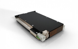
An example of an HPEC COTS [commercial off-the-shelf] processing module that leverages the new class of ACAP hybrid architecture FPGAs is Curtiss-Wright’s VPX3-536 Adaptable Processor, a high-performance SOSA aligned 3U VPX FPGA PIC module (Figure 1). The card is designed for use in demanding sensor-processing applications, including latency-sensitive radar, EW [electronic warfare], and signals-intelligence DSP.

[Figure 1 ǀ Rear view of Curtiss-Wright’s VPX3-536 FPGA engine with VITA 66 fiber optics.]
The hybrid devices can help meet demand for SWaP-optimized, SOSA aligned HPEC radar and signal-processing parts while leveraging the potential of AI/ML to improve image recognition.
Mike Southworth is Senior Product Line Manager, C5ISR, for Curtiss-Wright Defense Systems.
Curtiss-Wright Defense Systems https://www.curtisswrightds.com/