Reverse engineering for board test
StoryOctober 22, 2009

Kris Carlson
Seica USA
Bernd Hauptmann
Seica USA

Historically, customers are faced with situations where CCA data is not available for a variety of reasons. Situations where Original Equipment Manufacturers (OEMs) have been acquired by other OEMs or designs have been generated prior to the age of remote storage or escrow agents can result in the loss of data. Some companies, especially market segments such as depot repair, no longer have access to actual CAD or memory disks containing the original design files or source code of a particular CCA. With contract obligations up to 20 years, what can a field repair shop or depot do to create documentation for a particular CCA? The answer lies in utilizing ATE flying probers particularly designed to ?reverse engineer? a CCA. Reverse engineering can assist the depots in documentation creation and full test functionality.
In the electronics industry, “reverse engineering” is normally defined as the process of discovering the technological principles of a device, object, or system through the analysis of its structure, function, and operation.
Within electronic board test with Automatic Test Equipment (ATE), if the documentation normally required to generate a test program – for example, CAD data, schematics and BOMs – is missing, a reverse-engineering process based on a “gold” sample board can be used to recreate enough information (netlist) to generate a comprehensive test program with a reasonable amount of test coverage.
This program, created in a very short time and without the need for a complete knowledge of the functions of the Unit Under Test (UUT), can be very helpful when repairing faulty boards coming from the field, or when used to filter good and bad boards from an unknown batch of boards. A double-sided flying probe tester, equipped with a suitable set of dedicated software tools, can be the best solution to perform both reverse engineering and test, combining visual inspection capabilities and net-oriented vectorless test methods.
Reverse engineering test
To prepare a flying probe test program, CAD data is normally mandatory, together with a reasonable set of documentation (gold sample, BOM, schematics) of the UUT. With this information, which is almost always readily available in the case of currently manufactured products, the Automatic Test program Generator (ATG) automatically creates the program, applying the appropriate measurement techniques included in the software platform. The situation may be completely different in the case of boards coming from older products, which return from the field and must be repaired. Here, the documentation is often partly or even completely unavailable.
If the CAD data is not available, then important information is missing, such as the XY coordinates of the Test Points (TPs), the net list (electrical network of the UUT), and the parts list/BOM (values, tolerances). This, at first, may seem an insurmountable obstacle to the creation of a useful test program.
How can a flying probe tester be used to rebuild the netlist (and the part list/BOM) and then test an electronic board when the documentation is missing?
The solution
As already addressed, the XY target coordinates for the individual test points (TPs) can be directly learned by using the cameras available on each side of a double-sided flying prober. Once these coordinates are known, the netlist can be directly extracted by using the flying prober, with the help of special measurement methods. With these so-called “net-oriented test methods” a parts list (BOM) is not necessary. Only a gold board is required.
We will first take into consideration the test methods used with the reverse-engineering process and then the procedure.
‘Net-oriented’ flying probe test methods
Fnode
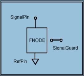
Fnode is a dynamic impedance measurement method, which acquires the net signature of an analog bi-pole. This powerful test method (Figure 1) is used to measure the dynamic impedance of an unknown bi-pole, where pin 1 is a signal net of a UUT and pin 2 is a reference net (typically GND).
Figure 1: An Fnode is used to measure the dynamic impedance of an unknown bi-pole, where pin 1 is a signal net of a UUT and pin 2 is a reference net (typically GND).
|
|
Since each bi-pole of the UUT is unknown, an “autolearn” of a gold board is used to acquire the behavior of the bi-pole over a broad frequency range. A signal generator applies a frequency Sweep (Figure 2) to pin 1 while pin 2 is connected to GND (Figure 1). The typical input signal amplitude is 0.2 V so as to remain below the P-N transition threshold and to avoid nonlinear distortions, as well as to avoid guarding (electrically isolating the net environment to do an individual measurement on a single component).
Figure 2: Fnode: typical signal waveform. In green is the voltage applied between the net under test and GND; in red is the current signature of the net.
|
|

The Fnode technique measures the current, which flows into the bi-pole. In each case, the amplitude and the phase for each net is stored by the test program. Fnode is a purely passive measurement procedure, with no power on the UUT.
The advantages of Fnode are easily summarized: It is a purely passive measuring procedure that can be generated without CAD data, and no manual debug is necessary. The autolearn process runs automatically and creates a full shorts test with higher fault coverage than the traditional adjacency test.
In addition, many in-circuit measurements can be eliminated without decreasing test coverage.
This procedure utilizes a DSP-based (Digital Signal Processor) multifunction instrument, which digitizes the generated and measured signals. Because all of the test models are “hardware emulated,” the acquired data enables the almost simultaneous execution of multiple high-speed tests, substantially increasing test throughput.
PWMON
Once the analog signatures have been acquired during the Fnode procedure, we still need to acquire the signatures/functions of the digital components; the PWMON technique enables this acquisition. During this procedure, the UUT is powered on, and the current needed to produce logic 0 or logic 1 on each node (input pin of a digital component) is measured. Employing this learned threshold technique, the system can recognize a possible error on a net. Using this method, a gold board is not necessary, even though it is strongly recommended.
The advantages of PWMON can be summarized as follows: It is a vectorless method to test ICs in a powered-up condition and can be generated without CAD data. It does not require manual operations since it is a fully automatic procedure and is independent of UUT initialization conditions (when the UUT is powered on).
Sequence of operations required for reverse engineering for test
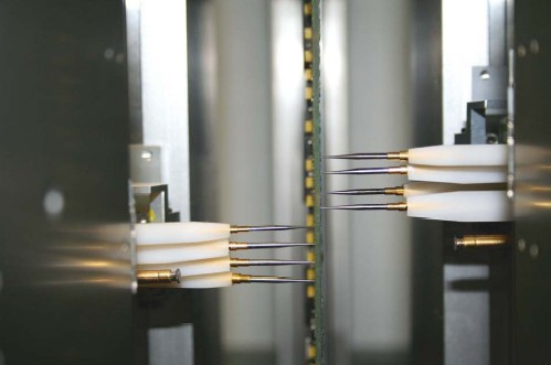
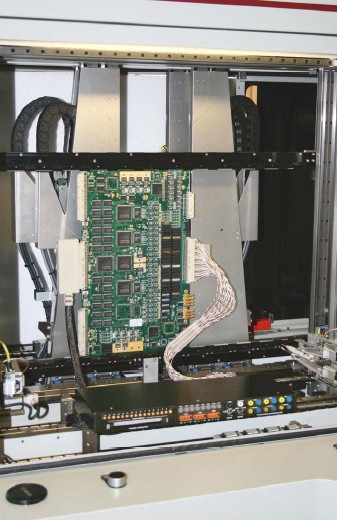
The first step is the acquisition of the image of the UUT. The gold board is clamped in the flying prober and with the use of the integrated CCD cameras and the digitizer option, the entire board image is scanned. Once the images have been acquired, the user can define, either on-line in the system or off-line on a remote PC, the XY target coordinates of all TPs (pads, pins, vias, and so on) through a simple point-and-click procedure.
If the main goal is only to test the UUT, it is sufficient to define the target coordinates only on one side (assuming that all nodes can be accessed from that side). If the goal is to recreate the schematics of the UUT, then the XY coordinates for all of the TPs, vias, pads, and pins on both sides of the UUT must be defined. Subsequently, the GND TPs must be manually identified before proceeding to the next step (Figure 3).
Figure 3: If the goal is to recreate the schematics of the UUT, then the XY coordinates for all of the TPs, vias, pads, and pins on both sides of the UUT must be defined. Subsequently, the GND TPs must be manually identified before proceeding to the next step.
|
|

Now the netlist learning process on the flying prober can be started, which assigns a unique net name to each target point, belonging to the same net and defining only one TP for each electrical node (Figure 4).
Figure 4: The netlist learning process on the flying prober assigns a unique net name to each target point, belonging to the same net and defining only one TP for each electrical node.
|
|
During netlist learning, the test system performs the following operations: first “autodebug” then the Fnode procedure on each individual target point. Afterward, different groups are built, which have the same identical signature. Continuity tests for each pair of targets belonging to the same group are conducted separately to make sure they belong to the same net. After the netlist-learning process, the targets belonging to the same net will have the same net name and only one TP per net is fixed for the next test operation.
A limitation to this process is low-value resistors (~5 ohms and less), low-value inductors, and normally closed relays, which appear as shorts (Figure 5).
Figure 5: A limitation of the netlist-learning process is low-value resistors (~5 ohms and less), low-value inductors, and normally closed relays, which appear as shorts.
|
|

Now we are ready for electrical test
After the netlist-learning process is complete, we can begin with the net-oriented test methods such as Fnode and PWMON. Since we know the XY coordinates for our test points and the UUT netlist (only the component information is missing at this point), we can move on to the next step.
The next step is to learn the “analogue signature” at all the TPs (one for each net) with the Fnode method, utilizing Fnode in autodebug. Subsequently, when running the UUT using the Fnode test procedure, possible short-circuits and similar errors at the UUT are detected.
At this point we have addressed the analog part of the UUT, and can now turn to the digital portion. Once the GND and VCC inputs have been identified on the UUT, we can connect a cable with supply voltages and the PWMON procedure can be started to detect possible digital faults on the ICs (Figure 6).
Figure 6: Once the GND and VCC inputs have been identified on the UUT, we can connect a cable with supply voltages and the PWMON procedure can be started to detect possible digital faults on the ICs.
|
|
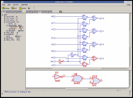
Once we have completed the previous step, we would be finished; however, only if we wanted to reach the “reverse engineering for test” stage. To continue the reverse-engineering process and recreate the technical documentation (for example, part list, schematics), the component information would need to be entered manually into the test program. Once we have entered the parts list, the test system can export the CAD data into an EDIF 200 format. Using special software tools, the schematics can be generated and printed (Figure 7).
Figure 7: Once we have entered the parts list, the test system can export the CAD data into an EDIF 200 format. Using special software tools, the schematics can be generated and printed.
|
|
Flying probers and reverse engineering
Flying probers are not only a flexible tool for board test. They can be very useful in reverse engineering, both for test and for recreating the technical documentation of the UUT. To enable the latter, the flying prober needs to be equipped with specific software and hardware characteristics and algorithms that enable the generation of a comprehensive test program without CAD data or parts and provide the necessary facilities for assigning test points and entering component information.
Seica, Inc./Seica Deutschland GmbH
603-890-6002
www.seica.com