Saving power and system cost with commercial parts qualified for space applications
StoryJune 15, 2020

Ken O'Neill
Microchip Technology
Organizations purchasing satellites are on a perpetual quest to extract ever-increasing value from space assets: We see operators of imaging satellites seeking higher image resolution, faster frame rates, finer channel resolution, and more channels to enable advanced multispectral and hyperspectral imaging.
As designers create imaging payloads with sufficient resolution to meet the needs of satellite operators, they encounter the perennial problem of constrained downlink bandwidth. It is impractical for low earth orbit (LEO) imaging satellites generating tens of gigabits per second of data and orbiting the earth roughly 16 times a day to send a constant stream of data to the ground through a space relay network.
Historically, imagery data was compressed and stored on board the satellite; however, more efficient use of the data relay network providing connection to the ground station can be accomplished by performing a greater amount of data processing on board the satellites so that information can be transmitted to the ground, instead of raw data. This change has driven an explosion in requirements for components capable of achieving the high rates of data processing needed while at the same time meeting stringent requirements for radiation tolerance.
Developments in the field of artificial intelligence and machine learning (AI/ML) have created some interesting opportunities to optimize the use of downlink bandwidth, for example by eliminating images that contain nothing of interest (for example, in a satellite that monitors land use, images in which the ground is obscured by thick cloud would be of no value; or in a satellite that tracks maritime traffic, images of the ocean in which no ships are visible). Further, the use of AI/ML allows for automated decision-making on board the satellite, thereby reducing or eliminating human analysis that can add days or weeks of latency to the deployment of imaging data.
As mission requirements evolve, there is a clear and persistent need for the latest technology in space assets; however, any product deployed in space needs to meet certain basic requirements for sustainable and reliable operation. The need to provide faster revisit rates for Earth-observation imaging drives requirements to field constellations of satellites, which in turn drives the requirement to lower satellite-acquisition costs.
To prepare a commercial component for use in space applications, three key steps are needed: radiation assessment, packaging, and qualification.
Radiation assessment
Radiation effects in space are pervasive and depend on the orbit. The deleterious effects of radiation effects on any component destined for space must be assessed, as radiation can cause physical damage to the part and consequent loss of operation of critical equipment of the satellite. Table 1 summarizes radiation effects in a variety of Earth orbits.

[Table 1 | Radiation effects in Earth orbit.]
Radiation effects in space are broken into two main categories: total ionizing dose (TID) effects and single-event effects (SEE).
TID refers to the long-term accumulation of radiation. In most microelectronic devices, TID causes performance to degrade and leakage current to increase. TID may even cause a complete loss of functionality. TID effects can vary with small variances in wafer-fabrication process, so microcircuits intended for space applications are often offered with TID testing on a per-wafer-lot basis. The successful deployment of any microcircuit in space depends on a complete understanding of TID effects for the devices being flown.
SEE refers to the outcome of the interaction of a microcircuit with a single subatomic particle. In space applications this is typically a proton or heavy ion, while in aviation applications is typically a neutron. SEE can be divided into several subcategories: single-event latch-ups, single-event upsets, single-event transients, and single-event functional interrupts.
Single-event latch-up is a phenomenon where a parasitic PNPN [anode/cathode] structure becomes forward biased due to the ionization caused by a heavy ion, conducting levels of current which can cause irreversible damage to the integrated circuit.
Single-event upsets occur in flip-flops and embedded memory elements due to the current pulse that results from the ionization and subsequent recombination of atoms of silicon when a heavy ion passes through a microcircuit. Several forms of mitigation are available to designers, such as triple modular redundancy (TMR) for flip-flops and error detection and correction (EDAC) encoding and decoding for memories.
While single-bit upsets in flip-flops or embedded memory cells may have limited consequences, they can be catastrophic if they occur in the configuration memory of a static random-access memory (SRAM)-based field-programmable gate array (FPGA). In this case, a single heavy ion can cause unintended changes of functionality of the FPGA (Figure 1, next page). Extensive system overhead in the form of configuration scrubbing and repair is needed to mitigate configuration upsets.

[Figure 1 | The effect of heavy ions on the functionality of FPGAs.]
Transient changes in signals caused by single-event radiation effects in combinatorial logic are referred to as single-event transients and can be problematic if the transient is present at the data input to a register at exactly the moment the register is clocked. In this case, the transient is preserved as a single-bit upset. As clock frequency increases, the probability of capturing a transient also increases.
Any single radiation event that causes a change in function of an integrated circuit is referred to as a single-event functional interrupt. As integrated circuits (ICs) become more sophisticated, the number of modes in which single-event functional interrupts can occur increases dramatically.
The successful deployment of any microcircuit in space depends on a complete understanding of radiation effects for the devices being flown. Therefore, it is important for organizations developing space-flight hardware to have test data for the exact wafer lot of the sourced flight parts. However, assessments of radiation effects require destructive tests; flight units cannot be tested for radiation effects as that would severely affect the expected lifetime of the parts. Testing for TID effects is done on a sample basis for each wafer lot. Testing for SEE is performed early in the product’s life, as SEEs are dependent on the integrated circuit design and tend not to be so variable with the wafer-fabrication process.
Extra caution must be taken with commercial parts as any shipment of commercial parts may be sourced from different wafer lots – maybe even different die revisions or even different foundries – which can dramatically increase the variability of radiation effects in the parts. Without strict traceability, it is impossible to be sure that the parts subjected to radiation testing are representative of the parts being flown. In contrast, microcircuits offered for space flight usually have complete lot traceability and the manufacturer of the devices can provide TID test data for the specific wafer lot sourcing the flight parts.
Packaging
Hermetically sealed ceramic packages are used for most microcircuits used in high-reliability satellites. There are three main reasons for the use of ceramic packages. The first relates to the inspectability of ceramic packages: Military standards governing the manufacturing and testing of components for use in space systems (for example MIL-PRF 38534, MIL-PRF 38535, and MIL-STD 883 class B) call for third-party inspection of the integrated circuit in the package prior to sealing the package so that the quality of the assembly may be verified. Inspection is readily performed in ceramic packages prior to lid seal.
Another advantage of ceramic packages is that in extreme temperatures or in a vacuum, the ceramic material does not emit vapors, a phenomenon known as outgassing. In contrast, plastic packages can emit vapors, which can cause fogging on optical components in space. The final advantage of hermetically sealed ceramic packages is that they can protect the microelectronic component inside against ingress of harmful moisture or board-cleaning fluids during assembly and integration of space-flight hardware.
For these reasons, hermetically sealed ceramic packages are required for the most stringent and highest-level missions, such as national-security space missions and human spaceflight missions.
Ceramic packages face some increasing and significant challenges as performance requirements increase. More I/O pins required by modern ICs requires that pins for signals, power supplies, and ground are mounted in a 2D array on the underside of the package, as opposed to a linear arrangement of pins around the outside of the package, as implemented in some traditional packages such as ceramic quad flat packs (CQFP). The mismatch of thermal expansion coefficient between package and board causes mechanical stress that can cause normal solder balls to shear as the printed circuit board (PCB) cycles through the extended temperature range. To solve this problem, solder columns are used instead of solder balls; solder columns are mechanically flexible and absorb the mechanical stress associated with the differing rates of thermal expansion of the board and ceramic package.
An additional challenge with ceramic packages is associated with their electrical properties. The latest on-board signal processing systems are being designed with serial data interconnectivity between ICs and between circuit boards, with data rates reaching into the 10 to 12 Gb/sec range. Ceramic packages can keep pace with these needs. However, the next generation of systems will exceed these data rates, which will challenge today’s ceramic package technology. Ceramic package suppliers are responding to the challenge with new technologies which are currently in evaluation.
Because of the challenges in using ceramic packages, some space programs are planning to use integrated circuits with plastic packages. Plastic packages have the advantage of lower electrical parasitics than ceramic packages, which enables higher performance in high speed I/Os. Additionally, the coefficient of thermal expansion of plastic packages is much closer to that of the PCB material, which dramatically reduces the mechanical stress on solder balls, eliminating the need for solder columns which promotes higher performance.
Qualification
The testing performed during qualification of an IC for space use depends on whether the IC is integrated into a ceramic or plastic package.
In the case of ceramic-packaged ICs, qualification is performed to an established standard such as MIL-PRF 38535 or equivalent ESA [European Space Agency] specification. Most U.S.-based suppliers will qualify to MIL-PRF 38535. Major steps of the qualification are listed in table 1. There are two levels of qualification specified in MIL-PRF 38535, known as QML [Qualified Manufacturer List] class Q and QML class V. QML class Q is intended for high-reliability defense applications, while QML class V is intended for the highest-reliability space applications. The primary differences between QML class Q and class V is that class V has the most stringent qualification requirements, such as a 4,000-hour high-temperature operating life test for the qualification sample, as opposed to 1,000 hours in the case of class Q.
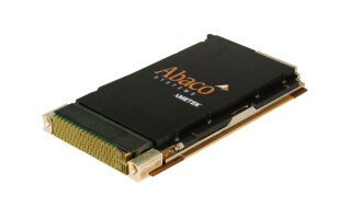
Examples of integrated circuits in ceramic packages are Microchip’s RTG4 radiation-tolerant QML class Q and class V-qualified FPGAs (Figure 2).

[Figure 2 | Microchip RTG4 radiation-tolerant FPGA.]
For integrated circuits in plastic packages, there is no agreement across the space industry on a qualification standard. Where plastic packages are offered for space applications, the qualification activities are based upon JEDEC Solid State Technology Association standards. Major suppliers and consumers of ICs in the space industry are collaborating on the definition of a QML standard for the qualification and screening of plastic-packaged ICs for space use, within the framework of a JEDEC committee. When a QML standard for space-grade qualification and screening of plastic encapsulated microcircuits has been agreed upon, it is likely that many IC suppliers currently supporting space-grade products will offer microcircuits qualified and screened to that standard.
New alternatives
Providers of satellite services are seeking to open new markets or create new capabilities – such as global communication networks and high-revisit-rate surface imaging – for which constellations of satellites are required. In order to keep the cost of deploying large quantities of satellites at a manageable level, the satellite designers often turn to components that are not designed specifically for radiation environments or space deployment. The risk in doing so is that commercial off-the shelf (COTS) components most often do not come with space heritage, space qualification, or even traceability or homogeneity of wafer lots, which means that radiation data gathered on one sample is not necessarily representative of the parts destined for space flight.
In response to this dilemma, some microcircuit manufacturers are offering radiation-tolerant components without the full set of QML space-level screening, for example in a plastic ball-grid-array package that is qualified under JEDEC standards. The development of a “Sub-QML” product such as this can offer an alternative approach that eliminates QML screening to save money. The use of radiation-tolerant microcircuits enables a high level of assurance and radiation heritage for space missions and avoids the lack of traceability seen with COTS components.
The evolving needs of space designers push the requirements for high-density, high-performance integrated circuits. The harsh nature of the space environment demands that a high level of radiation tolerance and high level of reliability assurance is available in components intended for space applications. Regardless of whether plastic or ceramic packages are used, a well-defined set of qualification and screening requirements needs to be in place to assure the success of future space missions. Established manufacturers of space-grade microcircuits are offering an expanded range of products including traditional QML-qualified components plus a category of Sub-QML devices that include the benefits of radiation tolerance and traceability, combined with lower-cost packaging and screening.
Ken O’Neill is associate director, Space and Aviation Marketing, FPGA Business Unit, Microchip Technology. He has supported FPGA applications in space, aviation, and other high-reliability markets for 25 years. Before joining Microchip and Microsemi, O’Neill served as a design engineer with Hewlett-Packard’s Computer Peripherals Group. Prior to that, he was a design engineer with Racal-Comsec Ltd. O’Neill holds a bachelor’s degree in electronics engineering from the University of Reading, England. Readers may reach the author at [email protected].
Microchip Technology • www.microchip.com