Optical and electrical high-speed communication in HPEC systems
StoryJuly 26, 2016

Thierry Wastiaux
Interface Concept

Throughout the defense field, demand for high-volume/high-speed data transfer for high-performance embedded computing (HPEC) is growing rapidly. Systems such as software-defined radio (SDR) use advanced, complex waveforms, all of which need fast sampling and generate huge amounts of data to be transferred. Other tools, such as active electronically scaled array (AESA) radar systems, generate huge amounts of data to be processed and transmitted.
High-speed transmission via boards and backplanes is starting to bump up against some physical limitations. Typical high-speed challenges include impedance mismatch, crosstalk noise, power and ground noise, and electromagnetic interference (EMI)/electromagnetic compatibility (EMC) performance. Impedance mismatches can occur due to line-width changes, vias, connectors, and cables.
Designers and manufacturers of printed circuit boards (PCBs) must monitor manufacturing tolerances carefully and ensure that such parameters as effective dielectric constant and surface-roughness variation are tightly controlled. Crosstalk noise is due to electromagnetic coupling between signal lines, via-to-via coupling, and digital/RF coupling. Power and ground noise control and tight requirements on the power distribution network (PDN) are essential to provide clean power to field-programmable gate arrays (FPGAs) and application-specific integrated circuits (ASICs). In particular, an imperfect power and ground delivery system results in simultaneous switching output (SSO) noise that propagates through the PDN. Moreover, most of the above effects produce EM radiation.
In order to design electronic boards with high-speed buses, designers can perform pre-layout signal-integrity analysis through software simulation using design-automation tools. Such a tool allows the user to define all the constraints for designing PCBs, including material, size of the stack, tracks and vias, anti-pads, stubs, and spacing between the tracks. Post-layout signal-integrity verification must then be performed. Electromagnetic simulation of the designed PCB enables extraction of the “scattering parameters” in order to verify compliance with VITA 68, which defines a VPX compliance channel. To improve impedance control and limit signal reflections, backdrilling techniques on the PCB can eliminate unwanted stubs; this process, however, makes the manufacturing process of the boards more complex.
Signal-integrity engineers today find that traditional electrical backplanes allow a data rate of as fast as 25 Gbps per differential link, provided that state-of-the-art techniques are used. The backplane connector remains one of the important limitation factors to reach this level. The industry is now under enormous pressure to develop new technologies, improve the performance of electrical transceivers, and define new standards and protocols to allow ever-higher throughput with lower energy consumption and smaller footprint.
One attempt to overcome these challenges is to use the fiber-optic technologies originally developed for telecom applications. These technologies are now brought to HPEC by designing rugged versions of the standard components that can operate safely in a wide temperature range. In this vein, VITA has approved the 66.1 standard covering fiber-optic connectors, and is currently working on finalizing the 66.4 standard, a variant covering half-width interconnects. Reflex Photonics and Samtec are among the companies currently designing small, low-power, rugged transceivers for use in HPEC designs.
These optical solutions are suitable for use in connecting the thousands of transmit/receive modules of the active antennas used in an AESA radar platform to the signal-processing system and more generally for connecting sensors generating important flows of data.
These optical fiber solutions are clearly one of the ways to dramatically push the limits of high-speed data transfer through VPX backplanes. Moreover, they are the most readily available to designers today, even when higher cost and need for rugged packaging is considered.
Signal-integrity engineers are now working on new technologies to try to push the data-rate limits on boards and electrical backplanes and further explore whether higher throughput could be achieved on classical differential links.
The current protocols largely use the NRZ (Non Return to Zero) modulation technology. Many protocols – for example, PCIe, 1000BASE-T, 1000BASE-KX, 10GBASE-KX4, 10GBASE-KR, and Aurora – are based on the NRZ simple modulation for their physical layer. Figure 1 tracks the power spectral density of NRZ, “T” being the NRZ symbol period, with one symbol corresponding to one bit.
Figure 1: NRZ power spectral density.
(Click graphic to zoom by 1.9x)
|
|

As serial data rates go beyond 20/25 Gbit/s per link – and to try to reach 40/50 Gbit/s – signal impairments caused by increasing bandwidth means that the high-speed serial data industry must shift its approach. Simple, baseband, NRZ signal modulation techniques are being left behind in favor of more bandwidth-efficient PAM4 (four-level pulse amplitude modulation).
PAM4 – which cuts the bandwidth in half by transmitting two bits in each symbol – must be distinguished from its symbol rate, referred to as Bd (baud). For example, a 56 Gbit/s PAM4 signal is transmitted at 28 GBd.
The only high-speed serial PAM4 standard that has been released so far is IEEE 802.3bj 100 Gigabit Ethernet (GbE), 100GBASE-KP4. To reach 100 Gbit/s total data rate, it combines four lanes at 13.6 GBd. The success of PAM2-NRZ has meant limited adoption of 100GBASE-KP4, but does provide a solid basis for the future of the emerging PAM4 standards.
Electrical PAM4 specifications will consist of multilane, low voltage, balanced differential pairs with embedded clocking and either transmitter or receiver equalization, or both. The increased impact of signal-to-noise ratio on PAM4 signals calls for forward error correction (FEC), which enables the maximum uncorrected bit-error rate (BER) to be increased to 10-6 for electrical signaling to achieve the data-rate targets, albeit at the price of some hardware complexity.
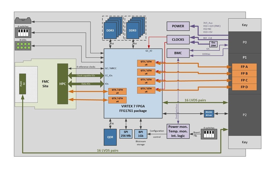
Interface Concept is using high-speed fiber-optic technologies for two purposes. One target allows the connection of many optical fibers to a VITA 57.4 FMC carried by Virtex-7 and UltraScale/UltraScale+ front-end processing boards. The IC-OPT-FMCa board can thus connect 12 Tx/Rx optical fibers to the high-speed transceivers of the last generation of FPGAs. This configuration offers a bandwidth of 480 Gbps on a small mezzanine board. Thanks to the backwards compatibility of the VITA 57 standard, this FMC can bring high-speed connectivity to VITA 57.1 as well as VITA 57.4 FPGA carrier boards. In the case of VITA 57.1, a maximum of ten fibers only can be connected depending on the number of high speed transceivers in front of the high-speed serializer/deserializer (SerDes) pins of the FMC connector. On the IC-FEP-VPX3c, eight fibers can be connected to two Quad Virtex-7 transceivers, as seen in Figure 2. In the second instance, designers are looking to overcome the throughput limitations of the VPX connectors and backplanes by implementing the solutions defined by the VITA 66 standard. As an example, a version of the Interface Concept UltraScale VPX 3U board features a VITA 66.1 connector for 24 optical fibers connected to six quad GTH transceivers on the FPGA and replacing the P2 VPX connector.
Figure 2: IC-FEP-VPX3c block diagram.
(Click graphic to zoom by 1.9x)
|
|
Simply put, when going well beyond 10 Gbit/s per differential link in a VPX chassis, the best short-term approach lies in using optical technologies. Looking farther out, it is clear that designers are reaching the limits of copper and that PAM4 modulation will be the basis of a believable path towards competitive 50 Gbit/s differential links.
Thierry Wastiaux is senior vice president of sales at Interface Concept, a European manufacturer of electronic embedded systems for defense, aerospace, telecom, and industrial markets. He has 25 years of experience in the telecom and embedded systems market, having held positions in operations, business development, and executive management. Prior to joining Interface Concept, he was responsible for the operations of the Mobile Communication Group and the Wireless Transmission Business Unit in Alcatel-Lucent. He holds an M.Sc. from France’s Ecole Polytechnique. Readers may contact him at [email protected].
Interface Concept www.interfaceconcept.com