High-speed ADC/DAC and FPGAs drive the design of next-generation SATCOM systems
StoryJuly 28, 2016

Denis Smetana
Curtiss-Wright
Many military satellite communications (SATCOM) systems operate in the very-high-frequency S-band (2 to 4 GHz) and C-band (4 to 8 GHz) range. Accurate sampling of satellite communications requires frequency rates that are at least twice, but preferably 2.5 to 3 times, the speed of the carrier frequency.
Many military satellite communications (SATCOM) systems operate in the very-high-frequency S-band (2 to 4 GHz) and C-band (4 to 8 GHz) range. Accurate sampling of satellite communications requires frequency rates that are at least twice, but preferably 2.5 to 3 times, the speed of the carrier frequency.
Until recently this proved beyond the capability of most conventional digital converter technology. For that reason, embedded systems designed to handle S-band and C-band transmission rates have typically required analog conversion techniques, such as frequency mixing, to convert the received signal to a lower fixed intermediate frequency (IF) to bring the signals within range of standard digital converter technology. The analog conversion requirement adds cost, complexity, and power requirements to these systems, none of which is desirable for deployed embedded systems.
A better solution would be to directly sample the signals using an analog-to-digital converter (ADC). In addition to eliminating the need for a front-end mixer, this direct sampling approach would also enable the full communications bandwidth to be processed digitally using digital signal processing (DSP) techniques.
Another challenge for embedded SATCOM systems is the large amount of processing required to fully process the generation and reception of SATCOM signals. Historically this has been addressed with expensive custom application-specific integrated circuits (ASICs) that can handle the system’s algorithms at the needed throughput. The good news is that as field-programmable gate arrays (FPGAs) have continued to grow in capability, SATCOM processing can now be performed using several FPGAs. This does require, though, that there is sufficient interconnect bandwidth (100 to 200 Gbps) to pass the data between the FPGA processing units. In addition to their lower cost compared to ASICs, FPGAs also provide reconfigurability, which simplifies and lowers the cost of upgrading the SATCOM system over time with new algorithms without having to change the system’s hardware.
Combining the advantages of multigigabit, ultrawideband sampling ADCs and DACs with today’s high-performance FPGAs now enables system designers to develop new classes of embedded SATCOM systems – for land-based stations or for simulation of space-based stations – that can sample and process S-band and C-band signals while eliminating the need to downconvert the signals using analog conversion.
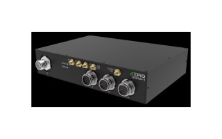
Making this development possible is the recent availability of open-standards modules that contain 12 Gsps and 25 Gsps ADCs and DACs, developed by Tektronix Component Solutions; these modules deliver the bandwidth required to directly sample both S-band and C-band signals. When integrated with FPGA-based OpenVPX modules, these devices enable the development of scalable SATCOM high-performance embedded computing (HPEC) systems that feature a reconfigurable architecture supporting updates via firmware. OpenVPX modules based on these devices may also be combined with other general-purpose processor modules, switch cards, or recorders to provide even more capability.
An example of a fully digital SATCOM system designed to handle S-band signals was recently developed by a leading SATCOM provider. (Figure 1.) The system uses the Curtiss-Wright CHAMP-WB-DRFM OpenVPX module, which combines both 12 Gsps ADCs and DACs and a Xilinx Virtex-7 FPGA. Because of the high amount of processing required, additional FPGA modules were used to pass data between the modules. The DRFM module provides 20 serializer/deserializers (SerDes) directly connected to the OpenVPX backplane from the FPGA. Since the SerDes can each run at rates up to 10.3 Gbps, they provided 200 Gbps of available bandwidth. An additional FPGA module with three onboard Virtex-7 FPGAs and 40 SerDes was directly connected to the backplane. The FPGA board’s SerDes, also running at 10.3 Gbps, provided 400 Gbps of available bandwidth. To provide more bandwidth, a rear transition module (RTM) was used to split the RX and the TX links into separate connections, enabling the Virtex FPGAs to use Xilinx’s simplex Aurora protocol in a unidirectional mode, so that each SerDes TX/RX pair did not have to go to the same module. Because the RX links can come from one card while the TX links go to a different card, the amount of SerDes bandwidth was effectively doubled when daisy-chaining the modules together.
The same concept may be applied to other wideband communication systems that use S-band or C-band frequency signals. The technique can also be applied to even higher rate signaling, where it enables downconversion that can’t be completely eliminated to at least be greatly simplified.
Figure 1: An example of a fully digital SATCOM system designed to handle very-high-frequency S-band signals.
|
|

Denis Smetana, Senior Product Manager, FPGA Products, Curtiss-Wright
www.cwcdefense.com