Denser networks, denser devices; the question is: how to test the I/O ports?
StoryJuly 08, 2008

Wayne Smith
Agilent Technologies

Advanced packaging and integrated circuit manufacturing techniques have resulted in multi-port devices that are difficult to characterize using traditional two- or even four-port Vector Network Analyzers (VNAs). A new class of test set extends the capabilities of the traditional VNA to N-ports, which provides full S-Parameter characterization of multi-port devices.
Denser integration and a trend toward using balanced I/O have increased the number of I/O ports on many devices such as network switches, bridges, and fabric muxes. While the overall performance of the assembly containing an integrated circuit device may improve compared to an earlier discrete component version, the performance of the individual components inside the IC is usually less than that of corresponding discrete components – particularly with regard to isolation. As a result, it is necessary to measure the effect of each port of a multi-port device, on itself and every other port on the device. This is done by measuring the S-Parameters for each two-port pair with all other ports properly terminated or error-corrected.
This would be a daunting task for a high-count I/O device if a two-port or even a four-port VNA were used since the number of single-ended S-Parameter measurements required is N2. For example, an eight-port device requires 64 S-Parameters to completely describe its single-ended behavior. Using an automated switch matrix would save time, but it would often degrade performance unacceptably. Manual testing could meet stringent accuracy requirements, but it would be unacceptably time consuming.
Figure 1
(Click graphic to zoom by 2.0x)
|
|

A new class of external test set that extends the port count of a VNA has evolved to meet multi-port testing needs. Commonly called N-port network analysis, where N is the number of ports on the device and the number of fully calibrated test ports, it uses internal switches and couplers to seamlessly integrate the test set with the VNA. This gives the N-port test set performance that is comparable to that of two- or four-port VNAs. Using N-port network analysis, the S-Parameters of any combination of port pairs on a multi-port device can be accurately measured with the systematic errors of all test ports and paths removed by error correction routines. Currently, 8-port and 12-port versions of N-port network analyzers are shipping, but there is no upper limit on the number of test ports that could be made available. Calibrating such an instrument would be time consuming if done conventionally, but fortunately techniques have been developed to greatly shorten the calibration process without compromising measurement quality.
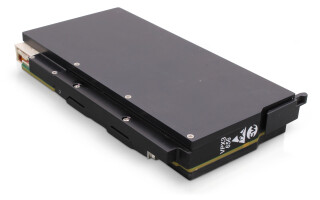
N-port network analysis has obvious application in R&D where it allows designers to quickly characterize a device and import the model into a simulation program. Similarly, production engineers are beginning to use N-port network analysis as an alternative to device-dependent test in production. Multi-port devices commonly require external components on some ports in order to operate. Often, "golden" components are built into test fixtures in production, which makes all test results dependent on those external devices. Using N-port network analysis, the multi-port device is first characterized and then functionally tested in simulation using ideal external components. The Agilent N5230A based physical layer test system (pictured) provides a high-performance and cost-effective solution for differential interconnect analysis. The novel instrumentation architecture enables faster measurements with a lower noise floor, thus providing faster design cycle times.
Wayne Smith recently retired from Agilent after 29 years of holding a variety of product planning and marketing positions. His most recent job was an aerospace/defense applications engineer in the Wireless Business Unit at Agilent Technologies where he focused on cellular technologies. For the past 11 years, that work has been exclusively focused in the area of RF and microwave products for the cellular and aerospace/defense market segments. Wayne graduated from the University of Nebraska in Lincoln with a Bachelor of Science in Education. For more information on this article, please contact John Barfuss at [email protected].
Agilent Technologies
800-829-4444
www.agilent.com