The next frontier: GaN HEMTs for high-reliability space and defense power architectures
StoryJune 16, 2026

Blake Soileau
Infineon Technologies
The space and defense industries face the critical challenge of delivering enhanced compute power in compact, efficient packages without compromising reliability or performance. In defense-related applications, in-orbit computing is the backbone of rapid-response superiority, enabling real-time imaging and communication. Gallium nitride (GaN) high-electron mobility transistors (HEMTs) are emerging as a transformative technology for these high-reliability sectors.
The pursuit of faster, more reliable, and consistent communication is driving an unprecedented surge in compute power demands. As global connectivity expands, power requirements are rising while design constraints tighten around form factor, efficiency, and rapid responsiveness.
In response, gallium nitride (GaN) high-electron mobility transistors (HEMTs) are emerging as a transformative technology for the high-reliability sector. GaN HEMTs offer superior efficiency and faster switching capabilities compared to traditional planar silicon (Si) MOSFET-based solutions, enabling the design of smaller, more efficient systems that meet the stringent demands of space and defense. GaN HEMTs can address pressing design challenges to empower the development of next-generation systems.
The power-delivery bottleneck
The modern defense and space landscape is defined by the need for rapid, real-time data processing. In satellite surveillance and tactical communications, the loop is particularly shrinking within sensor/image capture to transmission and reception. This change calls for in-orbit compute capabilities and requirements that were previously reserved for more traditional industrial and consumer-based applications.
With this compute surge comes a challenge in power delivery. From application requirements to hardware needs, today’s engineers are faced with a mix of obstacles, namely:
- Increased current demands: Next-generation FPGAs and processors require significantly higher operational and transient currents to operate with full functionality.
- Thermal constraints: These high-power devices must operate within sealed, vacuum-rated enclosures with limited convection cooling.
- Size, weight, power, and cost (SWaP-C) pressure: Launch mass and volume are at a premium. Bulky magnetics (transformers, inductors) and dealing with higher power losses (heat sinks, increased thermal layers) create additional size/weight directly penalizing payload capacity.
Traditional planar Si MOSFETs struggle to meet these demands without increasing system volume due to their limited switching frequency capability or adding more thermal solutions to deal with increased power losses. Engineers are now forced to choose between performance and reliability – GaN HEMTs offer a path to solve these constraints.
GaN is a wide-bandgap (WBG) semiconductor that fundamentally alters the power conversion equation. Beyond electrical performance, its physical architecture offers unique benefits for the radiation-hardened (rad-hard) environment.
Inherent TID tolerance
The primary failure mechanism for planar Si MOSFETs in space is the accumulation of trapped charge in the gate oxide layer due to total ionizing dose (TID). This leads to threshold voltage (Vth) shifts and eventual device failure.
GaN HEMTs utilize a heterojunction structure that operates without a gate oxide layer. Consequently, they exhibit inherent immunity to TID-induced threshold shifts. Characterization data indicates GaN HEMTs can withstand TID levels exceeding 1 Mrad (Si) with negligible degradation in Vth or RDS(on).
While TID tolerance is intrinsic to GaN’s internal structure, single-event effects (SEE) such as latch-up (SEL) or burnout (SEB), as well as new effects like single-event leakage current (SELC), still require design efforts to offer protection against these events. The removal of the oxide layer, however, simplifies the radiation hardening process compared to Si. (Figure 1.)
.jpg)
[Figure 1 ǀ Side-by-side comparison showing planar Si MOSFET (left) vs. a GaN HEMT (right). High TID tolerance results from the lack of a gate oxide in GaN HEMTs.]
Technical performance metrics: GaN vs. planar Si MOSFETs
For the power-design engineer, the transition to GaN offers quantifiable improvements across key power-stage parameters:
Increased efficiency and reduced heat:
- Lower RDS(on): GaN devices offer significantly lower on-resistance per unit area compared to Si.
- Reduced switching losses: The elimination of the body diode and lower gate charge (Qg) drastically reduces switching losses.
- Result: Power conversion efficiencies approaching 98%-99% are achievable with GaN. This reduction in heat generation enables smaller thermal interfaces and reduced thermal-dissipation surface area, directly lowering system mass.
High-frequency operation:
- Electron mobility: GaN’s high electron mobility enables switching frequencies in the MHz range, which exceeds the practical limits of Si MOSFETs, which is typically in the hundreds of KHz range.
- Magnetics reduction: Higher switching frequencies allow for a proportional reduction in the size of passive components (inductors, transformers).
- Impact: A 10x increase in switching frequency can reduce magnetic volume by up to 80%, enabling ultracompact DC/DC converters and isolated power supplies.
Improved thermal performance:
- Wide bandgap: The 3.4 eV [electron volts] bandgap enables GaN to operate at higher voltages in a smaller die area. This, combined with the electron mobility and electric breakdown field, means that GaN operates with lower power dissipation and less heat generation.
- Stability: GaN maintains stable Vth characteristics across a wider thermal range, reducing the need for complex temperature-compensation circuitry.
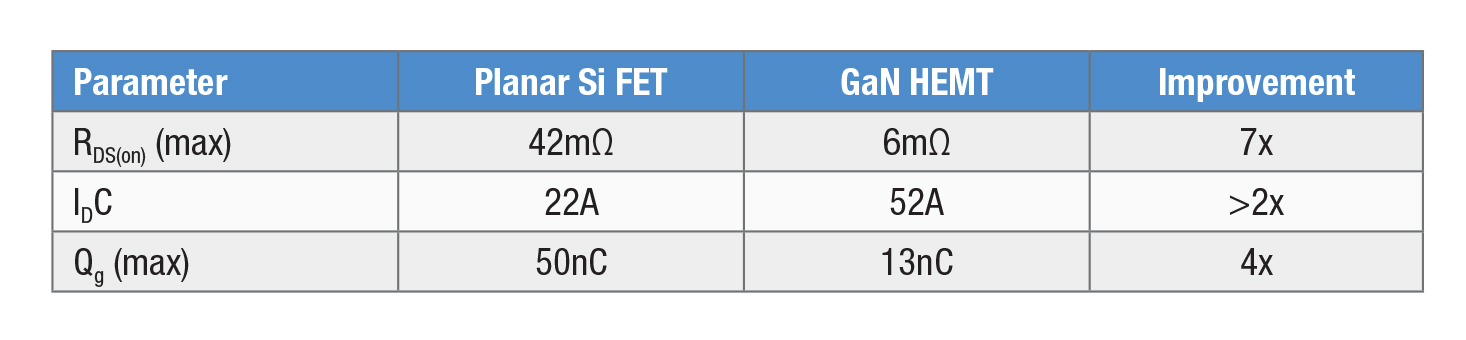
[Table 1 ǀ A table shows the relative comparison of a 100V N-channel planar Si MOSFET and a 100V GaN HEMT with the same die size. Significant improvements in RDS(ON) and Qg translate to increase current drive capability.]
Design implications for space and defense
Adopting GaN HEMTs is not merely a component swap; it is a system-level optimization. There are three significant advantages to GaN implementation: power density, thermal efficiency, and increased reliability. First, by shrinking magnetics and thermal management hardware, engineers can achieve 2x to 4x and greater power density (W/in³) compared to Si-based designs. Second, GaN’s simplified thermal architecture reduces heat dissipation, enabling the use of simpler and lighter thermal paths, crucial for cubesats and small satellite constellations. Third, the removal of the gate oxide eliminates a primary failure vector in the space environment, potentially extending mission lifespans and reducing the margin requirements for radiation hardening.
Integration considerations
Special care must be taken when transitioning to GaN-based system architectures. Key considerations include:
- Gate driver selection: Most GaN solutions are driven at lower voltages (~5V) compared to the 10V–20V often required for Si MOSFETs.
- Controller optimization: Drivers must be selected for optimized drive voltage and precise dead-time control to prevent shoot-through.
- Testing and characterization of SEE performance under all conditions: Effects such as angular sensitivity and flux dependency have a big impact on SELC. Is it critical that testing is done beyond previously established standards, written for Si MOSFETs, to properly stress and determine how GaN HEMTs will perform in-orbit.
- Understanding intrinsic and extrinsic failures to characterize low PPM failures: Understanding all potential failure mechanisms is critical to guarantee low target failure rates and ensure robust quality systems in-orbit. Relying on standards made for Si MOSFETs will not always capture extrinsic failures for GaN HEMTs, leaving gaps in understanding. Only with large scale accelerated lifetime tests can extrinsic and true device failure rate be determined
For design engineers tasked with developing next-generation space and defense systems, GaN HEMTs represent a high-reliability solution to the challenges of power delivery in an era of expanding compute requirements. By delivering superior efficiency, enabling high-frequency operation for smaller magnetics, and offering inherent TID tolerance, GaN allows for the development of compact, high-performance power architectures that meet the rigorous demands of modern defense and orbital applications. The technology is ready to move from the lab to the launchpad, empowering the next era of rapid-response defense systems.
Blake Soileau is a senior marketing manager at Infineon IR HiRel, covering the radiation-hardened portfolio for aerospace and defense applications. Blake has more than 15 years of experience in the semiconductor industry supporting a wide variety of roles within power-management products.
IR HiRel, an Infineon Technologies Company www.infineon.com/hirel