Unlock high-performance rad-hard FPGAs
StoryJune 14, 2023

Juan Garcia
Renesas
Today’s high-performance chips demand increasingly precise voltage tolerances on shrinking voltage rails and shockingly rapid, high-current load changes. In the satellite and space arenas, designers must also contend with the effects of TID [total ionizing dose] and SEE [single-event effects] on the output voltage accuracy of their supplies. Before choosing a power solution, designers playing in these spaces must create a regulation accuracy budget.
In an ideal world, a switching power supply can be set to output the precise voltage required to power a load, such as an FPGA [field-programmable gate array]. Under ideal conditions, if the input voltage or load current changes the output voltage will remain the same. Additionally, if the temperature changes, the output voltage will remain the same. This perfect power supply will even maintain a solid output voltage when exposed to radiation in space. In the real world, however, the output voltage of a real power supply will vary over all these conditions.
The output voltage errors can be categorized into a number of errors.
DC errors
DC errors arise from the reference voltage (VREF) accuracy, feedback resistors accuracy, line and load regulation, and PCB parasitic resistances.
Examining Equation 1 below, the key to ensuring the accuracy of the initial output voltage is to have an accurate VREF and feedback resistors values (RTOP and RBOT). The accuracy of the VREF primarily depends on the controller design. A good controller design will also minimize the error amplifier’s offset voltage (VOS) and input bias currents (IBIAS) to maintain an accurate voltage.
Eq. 1: ![]()
![]()
In addition to these sources of DC error are the line and load regulation. The line regulation refers to the change in output voltage in response to a change in the input voltage, while load regulation refers to the change in output voltage in response to a change in the load current. To minimize line and load regulation errors, the error amplifier’s open-loop (AOL) gain should be as high as possible. The final load regulation will depend on minimizing PCB trace resistances to the load.
AC errors
AC errors in a power supply include line and load transient response and switching noise.
Similar to line and load regulation, the line and load transient responses are AC changes to the output voltage in response to AC changes in the input voltage and load current. Minimizing the line and load transient response can be achieved using an error amplifier with high AOL gain, a fast control loop response, a good compensation network, and a good input/output decoupling capacitor network. The key to minimizing switching noise is using high-capacitance, low-ESR [equivalent series resistance] capacitors at a fast-switching frequency in the megahertz range, and an appropriate value inductor to minimize ripple current.
There are unique features for minimizing the load transient and switching noise that system designers can consider when selecting a switching controller for their power-supply design aimed at use in the high-radiation environment of space.
Temperature errors
Temperature errors include VREF drifting, feedback resistor divider drifting, and temperature drifts in the error amplifier, including bandwidth, gain, IBIAS, and VOS. These errors are caused by temperature changes in the IC [integrated circuit] die.
Looking at Equation 1 again, it is apparent that if the VREF and feedback resistor values change with temperature the output voltage will change. Datasheets typically provide information on the change in VREF over temperature. Some companies will include the errors caused by the error amplifier’s IBIAS and VOS changing over temperature. Lastly, the resistor divider temperature drift can be determined by reviewing the resistor datasheet.
Total ionizing dose errors
Total ionizing dose (TID) errors – the abundance of high-energy particles a part will be exposed to in space – include VREF drifting as well as the error amplifier’s bandwidth, gain, IBIAS, and VOS changes. These errors are caused by the cumulative effect of energetic particles depositing trapped, positive charges in the oxide and interface regions of the IC.
Datasheets for radiation-hardened parts will specify parameter limits over total radiation dose. Additionally, radiation-hardened IC providers will typically perform radiation lot acceptance testing to ensure the performance of their ICs over TID radiation.
Single-event effect (SEE) errors
SEE errors include latch-up, burnout, functional interrupt, and transients on the output of an IC, which are called single-event transients (SETs). SEE errors are caused by a single heavy ion depositing energy in a sensitive area of the IC.
Radiation-hardened IC providers will publish reports detailing the performance of the IC in a heavy ion environment. The reports also detail how often the IC might experience a functional interrupt or a transient in a heavy ion environment and how those events affect the operation of the IC.
Regulation accuracy budget analysis example
It’s important to figure out all the sources of error a power supply will experience, because most high-performance ICs such as FPGAs will have specific requirements and tolerances for each of its rails. As an example, let’s look at a controller for a power supply that can supply a max DC load of 135 A, at load transients up to 35% of DC load with a 200 A/µs slew rate, while maintaining ±4% accuracy over temperature, radiation, life, etc.
To start: Budget for a DC error of ±1% and AC errors of ±2% as an assumption. Subtracting these from the worst-case accuracy leaves a tolerance of ±1% for shifts caused by temperature, SET, and TID errors. The initial voltage regulation budget analysis is shown in Figure 1.

[Figure 1 ǀ An initial voltage regulation budget analysis is shown.]
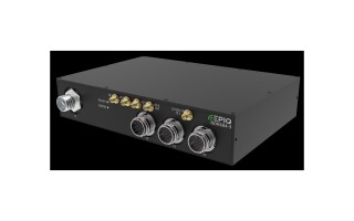
Regarding the choice of a controller, the ISL73847SEH PWM (Figure 2) is designed is designed for low-voltage, high-current applications such as the core rail of high-performance FPGAs.

[Figure 2 ǀ Shown: the layout of the ISL73847SEH controller.]
Its ±0.67% VREF tolerance across temperature, radiation, and life includes the error amplifier’s VOS. The line and load regulation for this part is a little less than ±0.25% over temperature. This overage can be attributed to the feedback resistor divider values and temperature drift; ±0.1% tolerance feedback resistors are recommended.
The ISL73847SEH supports a switching frequency range from 250 kHz up to 1.5 MHz. The higher switching frequency will help minimize the switching noise. To further reduce the switching noise while still addressing the high load current needs of the FPGA core rail, designers can turn to a multiphase configuration, which the ISL73847SEH can support. Using a 5 V input rail for a VOUT of 0.8V gives a duty cycle of 16%. Two phases brings a 15% reduction in ripple current, with 50% for a four-phase system and around 90% for a six-phase system. A four-phase system will also be able to provide 200 A DC max current, with ±0.25% of switching noise allotted to the budget.
On its evaluation board the ISL73847SEH has a peak-to-peak transient response of ~100mV for a full-load step of 900 A/µs. These numbers can be reduced by almost 50% by adding a resistor between the DROOP and VREF pins, a feature called droop regulation. In addition, ±2% can be allotted to load transient response.
From a radiation perspective, the part is high-performing, with no SETs up to a linear energy transfer (LET) of 86MeV cm2/mg and little to no parametric shift over TID.
The final regulation budget analysis is shown in Figure 3 for the ISL73847SEH, using droop regulation and a four-phase configuration. Notice how savings in temperature, radiation, and life errors enabled an increase in the budget for AC errors by ±0.25% (transient and switching noise), with ±0.58% margin leftover.

[Figure 3 ǀ Shown: The final voltage regulation budget analysis using the correct controller.]
Juan Garcia has been an applications engineer for Renesas Electronics for four years, working in the Radiation Hardened Space Products Group. His focus areas are DC-DC switching and linear regulators.
Renesas Electronics https://www.renesas.com/us/en