Hermetic power packaging vs. PEMs for mil electronics: No power issues here
StoryJuly 27, 2011

Alice Moss
Military Embedded Systems

In the midst of the debate over hermetic packaging versus Plastic Encapsulated Microcircuits (PEMs) in mil electronics, Microsemi quietly yet confidently recently announced a full line of new and re-released military-level-upscreened PEMs incarnated (or reincarnated) as TVSs, MOSFETs, IGBTs, and rectifiers. An interview with Shane O'Donnell, Microsemi's Hi-Rel Plastic Devices Program Manager
Remind us about Microsemi – its technology focus and areas of expertise, locations, number of employees, and goal in the industry.
O’DONNELL: Microsemi is focused on providing technologies where power matters, security is non-negotiable, and reliability is vital. Our key markets are defense and security, aerospace, enterprise and commercial, and industrial and alternative energy. Our solutions focus on differentiation in power, security, reliability, and performance and include high-performance, high-reliability analog and RF devices, mixed-signal and RF integrated circuits, configurable SoCs, FPGAs, and complete subsystems. Microsemi headquarters are located in Irvine, Calif., and [the company] has approximately 2,800 employees in the U.S., Asia, Europe, and India.
Microsemi recently announced a new line of plastic upscreened Plastic Encapsulated Microcircuits (PEMs). Which types of products are we talking about?
O’DONNELL: The new products and packages available for upscreening include MOSFETs, IGBTs, and rectifiers in D3Pak, TO-220, TO-247, TO-264, and SOT-227 packages. For some of the transient voltage protection (TVS) products, this could be considered a re-release because of die and assembly location requalifications.
What was the impetus?
O’DONNELL: Upscreened PEMs will provide the industry with a broader selection of products than is currently available strictly from hermetic packages. For example, when used in a transient voltage protection application, PEMs are available with large exposed copper bottoms and top clip technology that can be soldered directly to a heat sink. During multisurge incidents, getting the heat out of the package is imperative. So these features provide ultra-low thermal resistance (< 0.2 degree C/W) junction to case, and products in this package can handle surge currents in the 15-30 kilowatt range. Through-hole hermetic packages offering the same power rating have much higher thermal resistance, in the range of ~ 20 degrees C/W junction to lead.
Another example is MOSFETs. Hermetic MOSFETs are typically offered in a Breakdown Voltage Drain to Source (BVDSS) range of 100 to 500 V. However, these new upscreened PEMs are offered in the 800 to 1,200 V range. In addition, generally speaking, PEMs can offer smaller X-Y footprints, a lower profile, lighter weight, and other extended parametric ranges as compared to hermetic packages. Favorable pricing is always a factor, but that’s dependent on the amount of screening performed.
That’s quite a difference. Can you explain technically what the 5 types of upscreening tests on this new line entail?
O’DONNELL: The type of tests performed to the upscreened devices target various quality levels that utilize military testing techniques based off of MIL-PRF-19500. Table 1 provides an example of a standard transient voltage protection device (SMBJ36CA) upgraded to four reliability levels. To change the screening level, you change the prefix. By adding an “M” prefix, you obtain a device that includes process control. By adding an “MA,” you obtain avionic grade screening along with process control, and so on. The tests conducted for each level are shown in Table 2 as well.
The M prefix in the TVS product range represents a controlled process, where all aspects of the device production and test are controlled by Microsemi. Customers are informed of any change in this process even if the form, fit, or function is not changed. Lot-norming ensures all parts are within a close distribution of the average, and 100 percent surge testing verifies the clamping voltage specifications in the datasheet are adhered to.
MA products provide the optimum COTS+ offering with minimal device mortality levels. The MA upscreening flow offers ten -55 °C to +150 °C temperature cycles followed by three surge tests, 24 hours of high-temperature reverse-bias testing, three-sigma lot-norm screening performed on standby current, and final electrical tests.
The MXL TVS devices undergo more temperature cycles, surge tests, and a longer reverse-bias test. The parts also receive PDA evaluation and delta calculations with conformance inspection based on MIL-PRF-19500 Group A. MX devices receive all of these tests in addition to Groups B and C conformance inspection based on MIL-PRF-19500 specifications. The MXL MOSFET, IGBT, and rectifier devices get a 24-hour stabilization bake followed by various temperature cycling and high-temperature tests depending on the part type. Final electrical tests are always performed prior to dispatch, ensuring the parts have remained within specification.
Table 1: Upscreening data relative to part numbers and military equivalents
(Click graphic to zoom by 1.8x)
|
|
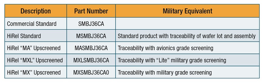
Table 2: Screening options for Transient Voltage Suppressors (TVSs) and MOSFETs, IGBTs, and rectifiers
(Click graphic to zoom by 1.9x)
|
|

Plastic parts are known for moisture ingress. How does your upscreening processes thwart this specific danger?
O’DONNELL: For harsh environments, hermetic packages will always have a place in high-reliability applications. A hermetic package in the context of microelectronics implies an airtight seal that will keep moisture and other harmful gases from penetrating the sealed package. For PEMs, steps can be taken to reduce moisture ingress and tests can be added to ensure the barrier of the package. Defect-free passivation of the surface of the silicon die effectively blocks moisture access to microchip devices. Designing the lead frame for epoxy adhesion and lock minimizes the effects of moisture. Choosing the right epoxy can enhance the resistance to moisture penetration. Moisture penetration tests are performed to establish the Moisture Sensitivity Level (MSL) of each type of PEM. Standard qualification tests performed on upscreened PEMs include testing at 85 percent humidity/85 degree Celsius (85/85) and autoclave or pressure pot testing. Moisture measurements are then taken after testing to ensure package integrity.
What percentage of military-specific products does Microsemi test?
O’DONNELL: PEM screening includes the same rigorous 100 percent testing as is applied to our hermetic package devices.
For which types of military applications/systems might this new upscreened product line be suited? Why?
O’DONNELL: PEMs are used where size, weight, performance, and various grades of reliability are needed. Two big users are Unmanned Aerial Vehicles (UAVs) and Unmanned Ground Vehicles (UGVs). Missile systems are another example where size and weight play a critical role in the design. These vehicles and systems may be unmanned, but a malfunction at the wrong time can cost lives. Other applications include ground-based military systems such as radar, vehicle, and telecom systems.
Where and when will the new and re-released upscreened military-suitable PEMS be manufactured and upscreened?
O’DONNELL: Die fabrication and package assembly will be performed at onshore and offshore locations utilizing Microsemi Corporation facilities and contract manufacturing facilities. Screening locations are at the Microsemi facilities in Ennis, Ireland and Bend, Oregon. These products are available now.
Looking toward the future, what are some of the military-appropriate PEM technology trends immediately on the horizon, and why are they needed, technically speaking?
O’DONNELL: For a given device footprint on a circuit card, the engineering community continues to seek better performance, smaller size, and less cost. Discrete MOSFETs, TVSs, IGBTs, and rectifiers are used in power systems; to handle power for a given footprint, new surface-mount packages are being introduced such as the Plastic Large Area Device (PLAD) package. Until recently, only through-hole-type packages with multistacked die were available for high-surge applications. PLAD-type devices offer large die and an exposed copper bottom pad, contributing to an incredibly low package thermal resistance (< 0.2 degree C/W), which dissipates package heat without expensive cooling techniques. A smaller form of the PLAD-type package is currently under qualification at Microsemi.
OK, so wrapping up, which technologies will be needed in your sector of the defense arena in the next 5 to 10 years, and why?
O’DONNELL: With the cost of energy continuing to rise, saving power will continue to be important. The development of wide band gap materials such as SiC and GaN for diode and FET switching applications will be the emerging, maybe even disruptive technologies of the future replacing silicon sockets. Wide band gap materials offer near zero conduction losses in switching applications. For example, we took measurements on a 40 W point-of-load converter with a 3.3 V output using GaN MOSFET switches and did a comparison against silicon MOSFET switches in the same circuit. We found an 8.5 percent improvement in overall circuit efficiency when using the GaN MOSFET switches. Both SiC and GaN base material costs are expensive today; but as more applications emerge, cost will come down, allowing for greater industry adoption.
Shane O’Donnell is a Principal Engineer and the Hi-Rel Plastic Devices Program Manager in Microsemi Ireland. Shane has more than 15 years of electronics design and development experience. His work includes power supply, microcontroller, and transducer circuit design in various medical products. He has a Bachelor of Engineering in Electronics degree from the University of Limerick. He can be contacted at [email protected].
Microsemi + 353 65 68 99724 www.microsemi.com